HDI Printed Circuit Boards - High-Density Interconnect PCB Technology
Over the years, electronic devices and gadgets have significantly reduced in size but increased in functionality. And most of it is possible due to HDI PCBs. High-Density Interconnector printed circuit boards have revolutionized the technical properties of devices and enabled manufacturers to add complex functionality without worrying about space restrictions.
Aside from reducing the weight and size of electronic devices, HDI PCBs have many other benefits. They also improve signal integrity and data transmission and thus are used in almost all devices nowadays. Let’s look at how HDI PCBs evolved throughout the years and the many benefits it provides us.
What Is HDI PCB?
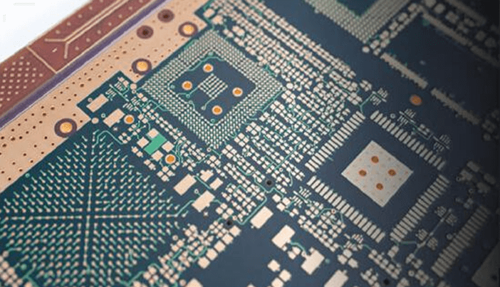
The HDI in PCB stands for High-Density Interconnector. It is different from the traditional printed circuit board in many aspects, but the most common among them are the fabrication and assembly processes. In traditional PCBs, the layers are connected through vias.
Vias are formed when holes are dilled mechanically on the layers, and copper is etched to make it conductive and connect the layers vertically. For complex or multiple layer PCBs, HDI PCBs are fabricated. Why? Because HDI PCBs have a higher wiring density on a smaller circuit board area, finer spaces, smaller traces widths, and high-density connection pads. This makes HDI PCBs ideal for complex or high-functionality devices with limited space.
There are multiple advantages of using HDI PCB, but first, let’s look at its history.
History of HDI PCBs
The evolution of HDI PCBs was made possible by the innovation and thinking of PCB and electronic devices’ designers and manufacturers. For example, the popularity of integrated circuits made designers and manufacturers think about mounting them to PCBs to get the most out of the new devices.
The BGA devices had very short leads for connection which made them ideal for reducing the size of the overall device. The main challenge was to convert the BGA devices from dual in-line assembly to surface mount assembly.
Next came the Chip-Scale Packages (CSP). These components were introduced with the hopes that the devices would be as big as the chip because of BGA devices' bottom connections. The intention was shifted slightly, and with the improvement of semiconductor manufacturing, the chip size was reduced, but the device remained the same.
Another improvement that further led to the advancement of HDI PCBs was Direct Chip Attachment (DCA). Instead of using traces to connect the chip pads to the PCB, DCA deposits the leads directly on the silicon.
In this technique, the devices are mounted upside-down on the PCBs. Currently, for HDI PCB manufacturing, via in-pad design technology is used. This design technique places the via directly under the device’s pad, making thermal and inductance capacity differences. The DCA and CSP work best with the via in pad technology and provide an optimum environment for smooth operation.
Benefits of HDI PCBs
Now that you know how HDI PCBs evolved, let’s look at some of their advantages in detail to understand their importance.
• The primary benefit of HDI PCBs is their ability to add more components on a single side. HDI PCBs utilize blind, buried, and micro vias to reduce the size of the components so they can easily fit together in a smaller area without space restrictions.
• The smaller size and higher number of components mean you can pack more functionality on a smaller device. Moreover, the signal path between the components is also reduced, thus improving speed and data transmission.
• HDI PCBs have higher wiring density and compact design. The compact size does not affect its performance and efficiency; instead, it provides a larger output than traditional PCBs.
• HDI PCBs also improve signal integrity. The use of micro vias and smaller traces reduces the time it takes for electrical signals to move between the layers and components. Moreover, it also reduces the device's capacitance and improves its performance and efficiency.
• HDI PCBs are more reliable than traditional PCBs as the layers are stacked on top of each other, protecting the core from external environmental factors and high temperatures.
• The design and manufacturing process of HDI PCBs has reduced the need to create prototypes for testing, thus making the PCBs readily available for market and increasing profitability.
HDI PCB Application
The many benefits of HDI PCBs make them ideal for use in multiple industries and devices. Let’s look at their applications.
• The miniaturization of the traditional PCBs makes HDI PCBs ideal for use in handheld devices like smartphones, tablets, laptops, and much more. They are also used in home appliances and computers.
• The manufacturing of HDI PCBs uses reduced voltage compared to traditional PCBs; this means heat generation is reduced and smaller batteries become sufficient. Moreover, the need for cooling fans has also been eliminated. Thus, HDI PCBs can easily be used in wearable devices, such as smartwatches, headsets, etc.
• HDI PCBs are used in devices that require higher signal transmission but have space limitations. They are used in lab equipment, diagnostic tools, CT scans, and more.
• HDI PCBs are also utilized in the aerospace industry. The resistance to extreme temperatures and high signal integrity make them ideal for defense and missile systems, aircraft, and more.
Future
The HDI PCB technology market is expected to increase with a CAGR of 8% by 2025. The trend of miniaturization is made possible with HDI PCBs, and they have multiple uses in the healthcare, aerospace, and consumer devices industries.
In the future, HDI PCBs will also be utilized in the automobile industry, enabling car manufacturers to add advanced functionality with improved signal transmission in a car without occupying much space. HDI PCBs can also be used in the IT communications and networking industry based on the various benefits they provide.
There are many variations of HDI PCBs. Thus, it's best to consult professional HDI PCB manufacturers, like Hemeixin, for consultation and a free quote.


