Why We Are a HDI PCB Manufacturer?
People and organizations belonging to fast-moving industries need to be informed about HDI (high-density interconnect) PCBs mainly because many of their rivals are already using and benefiting from it.
HDI PCBs allow you to increase the space on your PCB, which increases its efficiency and facilitates quicker transmission. Companies that integrate with HDI PCB manufacturers can easily see how these PCBs can prove beneficial for them.
Unsurprisingly, HDI PCB is perhaps the quickest-growing segment throughout the entire PCB market. Owing to the greater circuitry density, HDI technologies are capable of incorporating finer spaces and lines, small capture pads and VIAs, and greater densities in connection pads. HDI PCBs consist of buried and blind VIAs, and generally contain micro-VIAs with a maximum diameter of 0.006.
Benefits of HDI PCBs:
The advent of HDI PCBs has allowed engineers to enjoy greater flexibility and freedom in designing and manufacturing. Designers who use HDI approaches are able to integrate a greater number of components on either side of raw PCBs, if they have to. Essentially, HDI PCBs provide more space that designers can utilize, while simultaneously enabling designers to insert smaller-sized components within packed spaces. What this means is that HDI PCBs lead to faster transmission of signals, while also enhancing the quality of those signals.
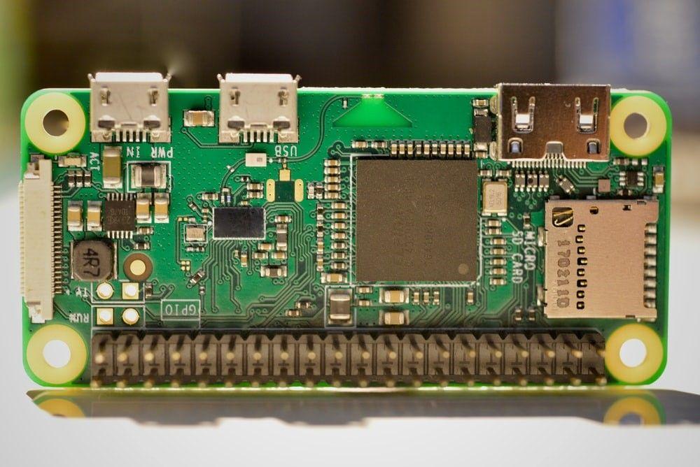
HDI PCBs are extremely popular, as they allow designers to lower the dimensions and weight of products, while also enabling them to boost the overall electric performances of electronic devices. For this reason, HDI PCBs are very common in devices such as touch-screens, mobile phones, digital cameras, laptop computers, and 4G and 3G network communications. Other than that, HDI PCBs often feature in various aircraft components and parts, as well as in a number of medical devices. An HDI PCB offers an endless amount of possibilities for designers.
Applications for HDI PCBs:
Like we mentioned, HDI PCBs offer many different kinds of possibilities, and are applicable across a range of diverse industries. As discussed above, it is common for you to find HDI PCBs in digital devices such as tablets and smartphones, where effective product application hinges on miniaturization. In addition, HDI PCBs are even used in aircrafts, automobiles, and any other vehicles which are in any way dependent upon electronics.
A critical industry for HDI PCB application is the medical industry. Medical devices often require a combination of strong transmission and small packages – a combination that is only creatable through HDI PCBs. For instance, the only way that an implant can be effectively adjusted in a human body is if it is small enough, but, at the same time, the electronics present in that implant must be capable of transmitting strong signals at high speeds. In such circumstances, an HDI PCB is nothing less than a godsend. Besides, HDI PCBs are quite useful in other kinds of medical devices and equipment, such as MRIs, CT scans, and monitors in emergency rooms.
Regardless of the industry that you operate in, you must be coming up with some ways that HDI PCBs can help enhance the quality or effectiveness of the electronics that you develop.
An HDI PCB needs reliable thin materials with high performance, along with thin lines and micro-VIAs with high density. Although the manufacturing process for HDI PCBs can be quite complex and intricate, the time, effort, and investment is extremely worthwhile, as the PCB’s reduced weight and increased compactness result in improved resistance to any kind of physical collisions.
HDI PCBs of Impeccable Quality:
Hemeixin has been offering HDI PCBs to its clients for a long time, and is one of the very first companies to have started offering this product. We make consistent investments to ensure that our HDI PCBs use fine-line, top-of-the-rank micro-VIA technology. Through our utmost commitment and experience in offering a comprehensive solution, we can address any design issues, reduce lead times, and ultimately deliver a product that is not just high-quality but also cost-effective.
HDI PCBs stretch the technological limits, and Hemeixin is proud to be at the very forefront of this innovation. Our team of skilled and dedicated engineers can adhere to even the most complex and rigorous requirements.
Through in-house laser drilling capabilities, Hemeixin attains precision and quality of the highest level. LDI (Laser Direct Imaging) ensures precise registration, while the AOI (Automated Optical Inspection) make sure that every inner core goes through a comprehensive check, highlighting even the slightest of defects present in the finest of features.
Final Word:
To sum up, we understand the benefits and applications of HDI PCBs, and the satisfaction that we attain from helping our clients improve their products is the core reason we are in the HDI PCB manufacturing business.
If you are considering implementing an HDI PCB in your products and want to learn more about how Hemeixin can help you in that regard, please feel free to reach out to us anytime. Our experts will be more than happy to walk you through the entire design process, as well as come up with an approach that will prove most beneficial for your products and business.


