What Is High-Density Interconnect PCB?
Consumer electronics have made tremendous progress in speed, performance, and power consumption over the last two decades, all while reducing weight and size. This has happened without sacrificing quality or functionality.
As the need for more powerful devices increased, it became necessary to discover a means to pack in more electronic circuitry into smaller and compact devices. HDI PCB Technology or High-Density Interconnect PCB is one of the major causes of this transition.
Various PCB manufacturers today, including HDI PCB manufacturers, develop a wide range of PCBs. It's a good idea to brush up on the fundamentals of PCB since it's impossible to avoid using them in your electronic projects.
It will be easier for you to identify a good manufacturer if you understand the basics of printed circuit boards. After all, what's the point of relying on a company that doesn't offer quality and affordable production rates? Keep reading to get down to the nitty-gritty of High-Density Interconnect PCB.
What Is High-Density Interconnect (HDI) PCB?
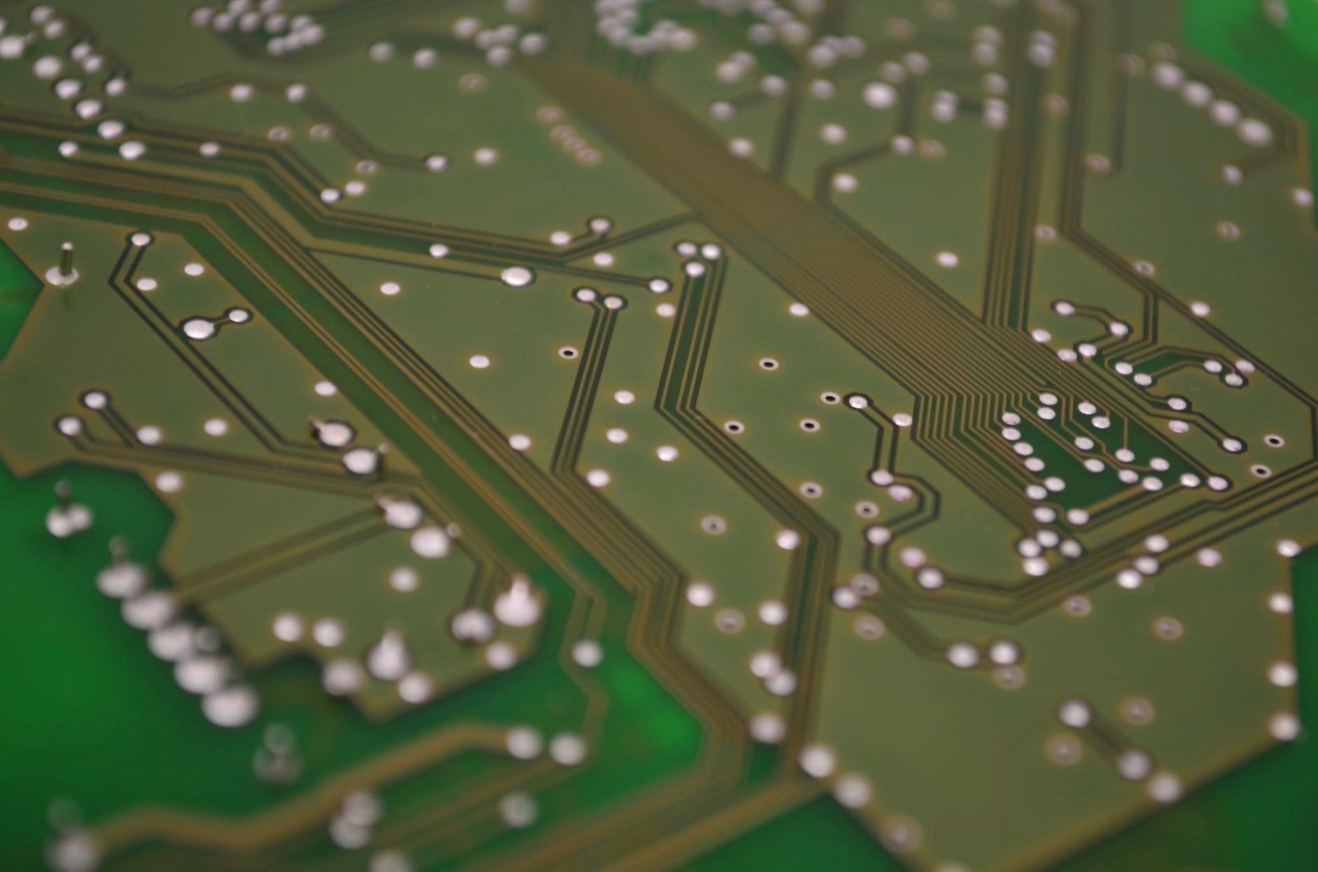
When it comes to the wiring density of circuit boards, the High-Density Interconnector Printed Circuit Board (HDI-PCB) is a preferable alternative. Due to their advancement, there are more refined lines, smaller vias, and connection pad density in HDI printed circuit boards. These boards are the go-to option for most buyers for improving electrical performance while simultaneously reducing the size and weight of their equipment.
HDI is an excellent option if the goal is to buy laminated and high-layer count boards. There is enough power on the PCB to handle high-speed signals. It has several properties, including reduced radiation, impedance control, and transmitting high frequencies. Electronic components have been arrayed and miniaturized, resulting in a high-density board.
In simple words, an HDI printed circuit board is designed to fit as many components as possible to ensure optimum performance.
Types of Vias in HDI PCB
HDI PCBs use vias, tiny conductive holes, to link various layers and allow signals to pass freely. Microvias, Through-Hole Vias, Blind Vias, and Buried Vias are all sorts of vias drilled into HDI PCBs, depending on the PCB's function.
Micro Vias are the smallest laser-drilled vias under 150 microns in diameter. HDI PCBs use microvias to connect one layer of a PCB to the next since they have a far smaller diameter than mechanically drilled vias like Through-Hole. The smaller design allows denser printed circuit boards to connect to one layer.
Through-Hole Vias are simple to create and the most cost-effective vias. They are further subdivided into Plated Through-Holes (which have copper pads) and Non-Plated Through-Holes (which do not have copper pads). The hole is drilled through the PCB from top to bottom using a drill or laser that connects all of the layers of the multi-layer PCB.
Blind Vias is a sort of via that is formed by drilling a hole through the external layer of the board and into the internal coating of the board. Blind vias in multi-layer HDI PCBs are called "blind" because the hole can only be seen from one side of the printed circuit board. However, constructing this form of the route is time-consuming and expensive.
Buried Vias is located within the printed circuit board and cannot be seen from the outside; therefore, it is referred to as "Buried Via." There is also an electroplated hole in the buried through, which requires a separate drill file. An even number of layers are present in a buried route; for example, 2, 4, 6, 8, 10, and so on.
Types of HDI PCB Stack-ups
Fabricators can employ HDI PCB stack-up types I, II, III, IV, V, or VI based on the IPC-2315 standard from the Institute of Printed Circuits (IPC). Types IV, V, and VI are more expensive to manufacture and are usually not suited for high-density PCBs with routing and BGA breakout difficulties.
Although plated through vias aren't required for flex PCBs following the HDI standard, they might be used to differentiate
HDI stack-ups. PCB manufacturers often use one of these stack-ups when assembling boards with high-density packages:
• Standard Lamination (Vias or Plated Through-Holes)
• Sequential Lamination (Plated Through-Holes, Blind, and Buried Vias)
• Lamination Buildup (Microvias)
Why HDI PCBs are the Future of PCB Technology?
HDI boards are one of the most rapidly growing PCB technologies. These contain blind, buried vias, micro-vias with a diameter of 0.006 or less than 0.006 inches. In addition, as compared to typical circuit boards, HDI boards have a higher circuit density than the latter. With HDI, It is possible to reduce the amount of space, the number of lines of code, the diameter of via, and the board's width. Furthermore, the HDI PCB allows a layer count from 4 to 24 and thicknesses ranging from 0.4 mm to 2.8 mm, ideal for space-saving.
In simple words,
• HDI PCBs are packed on both sides (more components can be placed on small board surfaces).
• It reduces power consumption, allowing for longer battery life.
• It provides PCBs that are light in weight and smaller in size.
• It allows for transmitting signals at high speeds while maintaining high signal quality.
• It provides more room for mounting components.
Final Thoughts
To sum up, this technology, abbreviated as HDI (high-density interconnected), is quickly gaining popularity in printed circuit board design. HDI printed circuit boards (PCBs) have the potential to deliver a variety of benefits to the technology industry as a whole. After all, they reduce circuit board complexity, allowing them to perform more functions while occupying less space.
HDI PCBs are the finest choice for modern-day consumers; however, it is essential to choose the right manufacturer when looking for high-quality HDI PCB boards.
HemeixinPCB has exceptional expertise in designing, developing, and deploying Printed Circuit Boards (PCBs) of various shapes and sizes. Producing high-quality boards in a short period is made possible by our knowledgeable personnel and outstanding production team. The competence and experience to work on projects of any size are among our strengths.
Consider us to be your first choice for board makers. Visit our website for more information.


