What Is HDI PCB Design?
Miniaturization of electronic components is driving the growth of printed circuit boards towards an unimaginable level of sophistication. Following the success of PCB, HDI PCB has evolved into a quantum leap for the twenty-first century. This futuristic technology has positively impacted different industries during the last few decades.
Phew, that was a lot of information to take in. Don't worry; you don't need to be an expert to understand HDI PCB design. Keep reading to get down to the nitty-gritty of the High-Density Interconnect Printed Circuit Board (HDI-PCB).
What Is a Printed Circuit Board (PCB)?
Circuit boards (also known as printed circuit boards or PCBs) are the fundamental building blocks of most modern electronic devices where all components are assembled. From single-layered boards like those found in your garage door opener to complex six-layer boards of smartwatches and high-speed circuit boards in supercomputers and servers with 60 layers—PCB is everywhere.
Think of it as a laminated sandwich structure of conducting and insulating layers. It performs two distinct yet complementary tasks. The initial step is to solder electrical components to certain positions on the outer layers to secure them in place.
The second objective is to generate reliable electrical connections (and open circuits) between the component's terminals in a regulated way, referred to as printed circuit board design (PCB design). Electrical connections are made on each conductive layer using an artwork pattern of conductors, similar to wires on a flat surface—developed specifically for that conductive layer.
A rapidly emerging PCB technology is known as printed electronics, distinct from those mentioned above. Printed electronics circuits are typically very simple and affordable. They can reduce electronic packaging expenses to the point where electronic solutions can be developed to solve problems that have never been considered before. Their use in electronics for wearable applications and disposable electronic gadgets has increased significantly, providing numerous opportunities for innovative electrical designers.
What Is High-Density Interconnect (HDI)?
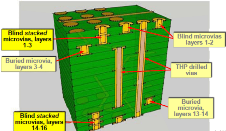
When it comes to the wiring density of circuit boards, the High-Density Interconnector Printed Circuit Board (HDI PCB) is a preferable alternative. Due to their advancement, there are more refined lines (less than 100 microns), smaller vias (less than 150 microns), capture pads (less than 400 microns), and connection pad density (more than 20 pads per centimeter squared) in HDI printed circuit boards. These boards are the go-to option for most buyers for improving electrical performance while simultaneously reducing the size and weight of their equipment.
What Is an HDI PCB Design/Layout?
The HDI layout comes into play when the traces on the PCB are less than 8 mils wide (0.2 mm). Since these techniques allow you to put more components on a single board, you can keep the size of your board small while increasing the number of components. Not all boards need HDI layout techniques, but some parts need them for proper routing.
An HDI PCB board requires smaller vias holes to move between layers. This is especially true for components with small pitches like BGAs. More traces per square mm need to be on the board. For fine-pitch parts, the HDI layout will often have the following features: smaller vias, thinner traces, higher layer count, and lower signal levels.
A Manufacturer's Advice on HDI PCB Design
High-Density Interconnection printed circuit boards, often known as HDI PCBs, are a form of technology that gained popularity during the twentieth century and is now utilized in various applications where the higher density is relevant.
An HDI PCB is always used in any device that requires increased computing power (such as a smartphone) while still being smaller and lighter in weight. However, even with access to such an advanced PCB, designers have difficulty developing a good PCB layout/design.
The designers must adhere to the general engineering technique of Design for Manufacturability (also known as DFM) for the best possible arrangement. It is a practice that encourages designers to make their designs quickly manufacturable. The more a device is manufactured at ease, the lower is the risk of future errors and the higher is the item's overall quality.
Always double-check with your manufacturer before starting a new design project that is more critical than HDI design. As mentioned above, not all designers have the same capabilities in this area; therefore, it's essential to check with your target manufacturer before creating an HDI configuration that can't be fabricated.
Maintain a tally of the distance between the traces and the pad. The same applies in the case of BGAs with a 1 mm pitch. The clearance criteria for the solder mask is typically the same size as the width of the trace that is being used. You can get a different solder mask clearance based on the pad size and pitch that you choose.
Do not utilize staggered vias or ELIC if you don't need to. The entire purpose of HDI routing is to give as much space as possible for routing on the surface and inner layers of the substrate. It may be tempting to layer the materials across the whole length of the substrate, but avoid doing so unless it is required.
Ensure you don't lose sight of signal integrity when working with an RF PCB board. All HDI layouts must be developed following high-speed design criteria or high-frequency guidelines. The same signal integrity standards in conventional PCBs apply to HDI PCBs; it's just a matter of scaling up the signal integrity rules.
Final Thoughts
We will summarize everything in one statement to make it easier for you to understand what we covered above: make every effort to improve the board's overall performance while simultaneously lowering the overall cost of the manufacturing process, if possible. That is precisely what a good PCB designer does.
As previously said, HDI layout and design routing necessitate the use of appropriate tools and collaboration with an expert design business. HemeixinPCB is your best bet. In addition to designing, developing, and deploying Printed Circuit Boards (PCBs) of various forms and sizes, they have extensive experience in manufacturing PCBs. Consider them to be your first and best choice for HDI PCB design. Visit their website for further information.


