Different Stackups for HDI PCBs
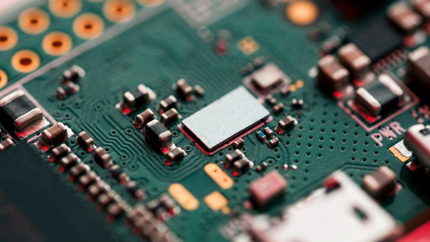
High Density Interconnect (HDI) PCB is a type of circuit board different from traditional PCBs, as it is smaller in size and can pack more components in a smaller area. You can optimize the size of the PCB without affecting its performance and flexibility. HDI PCBs are popular and in-demand nowadays because it has low power consumption and can pack more components while still keeping the device light. It also slows down thermal degradation and ensures maximum durability.
There are different types of stackup for HDI PCBs. But before we discuss them, let’s look at the three assembly approaches used by HDI PCBs manufacturers.
Assembly Processes
Each assembly process has its pros and cons, with cost building up for complex stackup types and manufacturing.
Standard
Standard lamination with plated through holes and vias costs less for 28 layers. If you have multiple large BGAs with less than 1mm pitch, routing would be difficult.
Sequential
Sequential lamination costs more than standard lamination. The sequential lamination with blind and buried vias has a simple model, shorter stubs, and smaller diameter than through-hole vias. Its reliability and minimum trace widths limit the number of layers you can add to the stackup type.
Lamination Buildup
Due to the limitations in the above two assembly processes, lamination buildup via micro vias is the best option. Micro vias PCB has smaller trace widths and vias with smaller dimensions, making it possible to achieve high routing density with reduced layers. By effectively using micro vias and placing them strategically on the circuit board, you can reduce the layers and increase routing space. It is the best method for designing large fine-pitch BGAs with pitch measuring 1mm or lower.
Micro vias are beneficial because they increase signal integrity, which is not possible if you are using typical materials. Also, the micro vias are not suitable with the standard and sequential lamination assembly method.
Types of Stackups for HDI PCBs
Depending on the assembly method, there are 6 types of HDI PCB stackups. Type I, II, and III are considered suitable, as the other three have expensive manufacturing and are not favorable for HDI PCBs due to fine-pitch BGAs.
The stackup types are differentiated based on the materials used, such as blind, buried, micro vias, and plated through vias.
HDI Stackup Type I
The HDI stackup type I has a single layer of micro vias on one or both sides, with a laminated core. It uses the stackup type buried and PTH vias, but not blind vias. It is not suitable for large dense boards with multiple pin-count BGAs because certain factors limit its performance. For example, to maintain reliability, the aspect hole ratio should be less than 10, whereas the FR-dielectrics are very thin, which makes it vulnerable to high temperature and causes delamination.
Also, if you use a single layer of micro via, then you cannot add multiple components or benefit from advanced features due to smaller and thinner diameters.
HDI Stackup Type II
The HDI stackup type II is better than stackup Type I for large dense boards with multiple fine pitch BGAs. It has a laminated core and is constructed using micro vias, blind vias, and buried vias. It requires a single layer of micro vias on both sides, or at least one.
Although there are a few limitations, the microvias can only be used in the outermost layer, thus restricting the use of power and ground plane layers.
HDI Stackup Type III
The HDI stackup type III is perfect for large dense circuit boards. It is also constructed using blind vias, micro vias, and blind vias, but requires 2 layers of micro vias on one or both sides. The micro vias are used on the inner layers; thus, manufacturers can add power and ground planes and improve signal integrity. Manufacturers can also stack vias, but that is expensive.
HDI Stackup Type IV
Not commonly used, the HDI stackup type IV doesn’t have any electrical properties and uses a passive core. It can be used for shielding, CTE management, and heat dissipation.
HDI Stackup Type V
This is another stackup type that is expensive to manufacture and rarely used. It has a coreless stackup and uses plated micro vias. All the layers are co-laminated and thus use a single lamination step.
HDI Stackup Type VI
The HDI stackup type VI is constructed using plated micro vias through sequential lamination or co-lamination. The conductive layers are made using antistrophic film and dielectric piercing.
i+N+i HDI Stackup Type
Following are the derivatives of HDI PCB stackup types:
● 1+N+1: this is a type II HDI stackup type. It consists of 1 build-up of high-density interconnection layers. The N refers to the number of layers, whereas the number itself refers to the copper foil on the top and bottom surface.
● 2+N+2: this is a type III stackup type. It is constructed using the sequential lamination assembly method and has two HDI layers on both sides.
● M+N+M: as the number of layers increases, the formula is used to calculate the number of layers. You can virtually create any number of layers of PCBs.
Based on the budget and the purpose of the device, manufacturers can use any of the above HDI stackup types, from I to III, to create the right HDI PCB for their project.
It's best to consult professional PCB manufacturers, like Hemeixin, for a free quote and consultation. They are experts in PCB prototype and PCB assembly and offer a full range of services like RF pcb boards, via-in-pad, laser-drilled microvias, and much more. They can provide you with the highest-quality HDI PCBs for your project.


