What is Any Layer HDI PCB?
Printed circuit boards are available in many types, and each consists of different layers. Depending on your project, you can choose between single-layer boards, multilayer boards, or flexible boards. Nowadays, High-Density Interconnect PCBs are most commonly used in electronic gadgets and consumer devices due to the ability to fit more components on a smaller board area.
HDI PCBs are miniaturized by using advanced technologies, such as stackup layers, smaller trace widths, and the use of a via-in-pad design. These techniques help improve signal integrity, reduce power consumption, and increase electrical performance.
This article will discuss derivatives of stackup types and their advantages and disadvantages.
HDI PCB Stackup Types
There are six stackup types for HDI PCBs donated by roman numerals, such as stackup type I, II, III, IV, V, and VI. Type I-III is considered suitable for high-density circuit boards, while type IV-VI is unsuitable due to costly manufacturing and assembly challenges.
There are also three derivatives of stackup types, which are important to discuss to understand how an HDI PCB is layered.
1+N+1
This is the simplest HDI stackup board design. It contains 1 build-up of high-density interconnection layer and is suitable for devices with multiple fine-pitch BGAs and lower I/O counts. It is made with fine lines, micro vias, and copper-filled via technology. 1+N+1 stackup type is extremely reliable and has stable mounting capabilities.
This stackup design finds use in cell phones, GPS, memory cards, and MP3 players.
2+N+2
This stackup board design consists of two or more build-ups of high-density interconnection layers. It is suitable for devices with smaller ball-pitch BGAs and higher I/O counts. Manufacturers can place the micro vias either in a stagger or stacked format. These structures are often used for devices that require high signal transmission.
The resulting board has a thin board with more space for routing. It can be used in video recorders, cell phones, and game consoles.
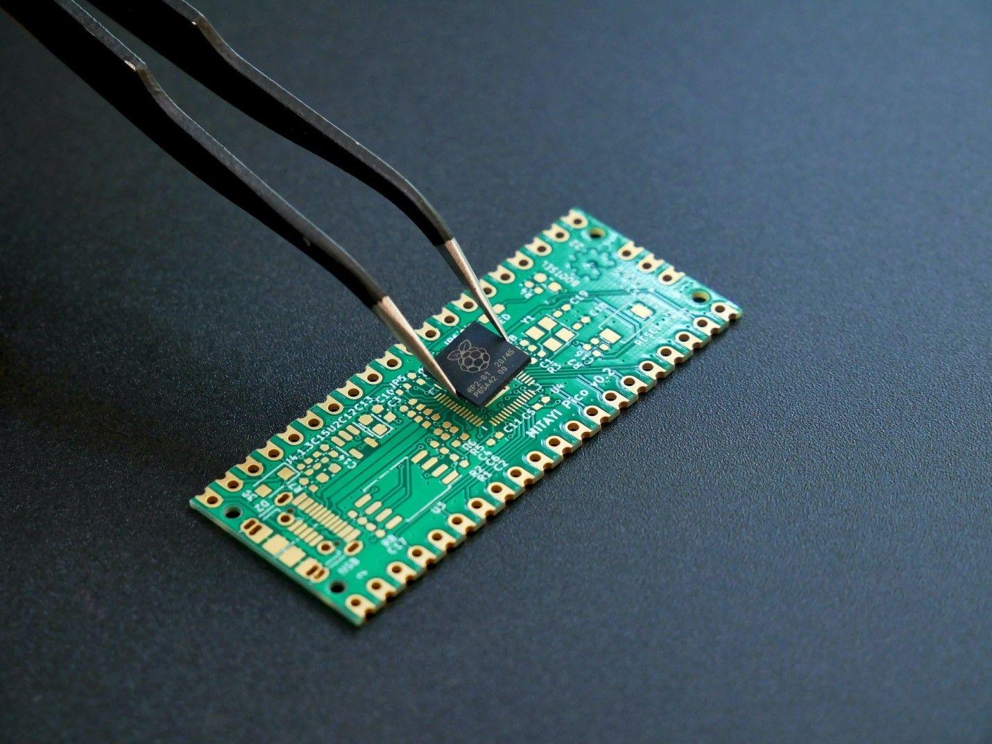
Any Layer PCB
This stackup board design is the next technological advancement of the HDI microvia PCB. Any Layer PCB enables free connection between layers by using laser-drilled micro vias in individual layers. The laser and filled-plating technology enable higher wiring density and design precision, ideal for miniaturized devices with many components.
It can be used for wearable devices, digital cameras, smartphones, mobile devices, and more.
Technology Used on Any Layer HDI PCB
There are special technologies used to build Any Layer PCBs:
• All available circuit board materials are suitable for Any Layer PCB.
• In mass production, minimum trace width and spacing are used.
• Microvias are stacked and copper-plated or filled with conductive paste.
• The edges are plated for shielding and protecting.
• Low DK material is used for mobile and consumer devices.
• Around 4 to 14 layers can be stacked up.
Other HDI PCB Layers
Many other layers make up an HDI PCB; let’s discuss them in detail.
Substrate Layer
The substrate layer gives the printed circuit board its rigidity and structure. Generally, most HDI PCBs are made from the fiberglass substrate layer. It is hard, rigid, and durable. Flexible HDI PCBs are made from a flexible plastic material called Kapton. Other material options include epoxies, although they are not durable and result in poor-quality circuit boards.
Copper Layer
The copper layer is next in line and is laminated to the printed circuit board using heat. The numbers of layers in multilayer PCBs are copper layers. For example, there is only one copper layer in a single-sided PCB. One side is used for conducting materials, and the other is used for placing electronic components.
As the layers increase, you have multiple surfaces to add functionality components. It also increases the routing density and decreases trace widths as you alternate between top and bottom layers.
The thickness of the copper layer also matters. If you want to create a high-power electronic device, you need to increase the thickness of copper layers.
Soldermask Layer
The solder mask layer is placed on top of the copper layers. It is used to insulate the copper layers and prevent exposure to other layers and materials that might disrupt its performance.
How to Determine the Number of Layers in HDI PCB
To determine what stackup type and how many layers are needed for your HDI PCB, you must ask yourself the following questions.
• What is your budget? Opting for a single or double-layer HDI PCB might seem cheaper, but it has limited functionality. You won’t be able to add advanced functionalities useful in today’s consumer devices. Multilayer HDI PCBs have costlier manufacturing due to higher layers, but it’s worth it.
• What’s the purpose of the HDI PCB? Think about which type of device you are developing and what kind of functionality it requires. If used in a complex high-tech area, you need a multilayer PCB.
• What parameters are necessary? Do you want an HDI PCB with higher signal transmission or controlled impedance?
• How many layers do you need? The numbers of layers depend on the pin density. For example, if the pin density is >1.0, you need 2 HDI layers, and if the pin density is <0.2, you need 10 HDI signal layers.
As mentioned above, the number of layers in an HDI PCB stackup depends on the pin density, the application, and operating frequencies. Increasing the number of layers improves signal integrity, reduces cross-talk and power consumption, and reduces electromagnetic interference.
As technology increases, so does consumer needs. Manufacturers now need to create consumer devices that are multi-functional, fast, and durable. This is possible through HDI PCB technology. Before designing a layout, it’s best to consult professional PCB fabricators like Hemeixin to choose the right HDI PCB stackup for your project. The stackup type can determine the device’s reliability and performance. We hope this article helped!


