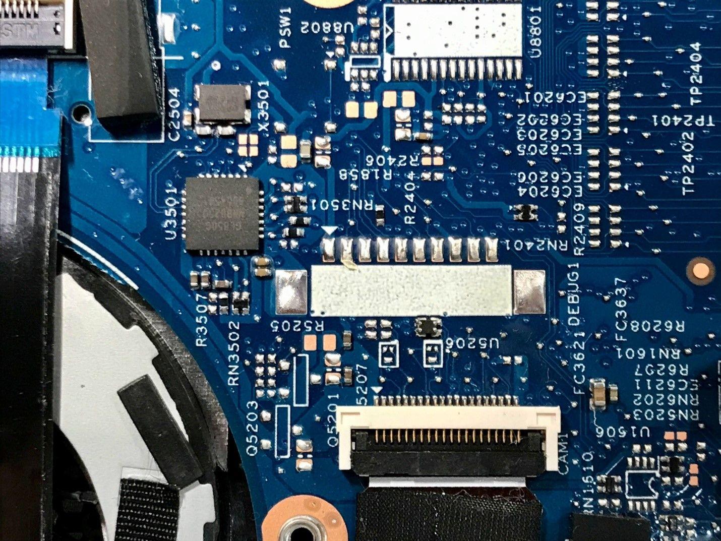
HDI Layout Guidelines for HDI PCB board
Besides size reduction, choosing HDI PCBs over traditional PCBs has multiple advantages. High-Density Interconnector circuit boards offer improved signal integrity and the ability to add more components on a smaller board. Thus, it has made possible the innovation of specialized smartphones and computers that we use nowadays.
The smaller size, lesser weight, higher wiring density, and multiple connection pads have made the HDI PCBs more reliable and fast. Thus, its use in healthcare, consumer devices, etc., cannot be ignored.
If you want to create an HDI PCB for your project that has a higher component density, you need to create an HDI layout first. The layout design process is complex compared to conventional PCBs and requires expert knowledge and skills. Let’s discuss the process in detail.
HDI PCB Design Layout Guidelines
When manufacturing an HDI PCB, not all circuit boards require a layout. The layout is only reserved for projects with a higher component density and needs to be fitted on a smaller circuit board, so the routing and spacing are perfect for reliable and efficient performance.
Some of the common practices you will find in an HDI layout are smaller vias, higher layer count, lower signal levels, and thinner traces. For instance, an HDI PCB uses blind, buried, or micro vias. These vias have a smaller diameter and are used for devices with fine-pitch components. Similarly, an HDI has a higher layer count and typically reaches up to 20 or more layers.
Besides these, a few do’s and don’ts in layout design can help you create the perfect HDI PCB layout.
• Depending on the pad size and pitch, the solder clearance values and the spacing requirements can vary. For 1mm BGA devices, it is best to use vias with a smaller diameter when the pitch falls to 0.8mm or more. Blind, buried, and micro vias are perfect for this purpose.
• Even though HDI PCBs have a higher layer count than traditional PCBs, manufacturers still recommend opting for fewer layers because higher layering makes designing and manufacturing complex and increases the project's overall cost.
• To ensure that the signal integrity and routing density do not get affected, you also need to follow some design guidelines for high speed. For example, give importance to trace spacing, limit the use of vias to prevent impedance discontinuity, use shorter trace lengths and equal length of pairs, etc.
• Don’t lay out your components across the entire substrate, and use as minimum space as possible for better routing.
Before you design an HDI PCB, it’s important to check if your manufacturer has the required skills and expertise to make it happen. Also, define a budget beforehand and work and design accordingly.
Besides these basic design guidelines, many other things are necessary for your High-Density Interconnector board layout. Let’s discuss them in detail.
Stackup Type
According to the IPC standards, there are 6 stackup types available for HDI PCBs. Types IV, V, and VI are considered unsuitable for HDI PCBs due to complex and costly manufacturing, so we will discuss types I, II, and III.
Stackup Type I
The HDI stackup type I is the most commonly used in HDI PCBs and is the cheapest to manufacture. In this type, manufacturers use blind and through-hole vias on both sides of the circuit board. It has only one micro via layer. One disadvantage of using stackup type I is that the layer count is limited due to the thick diameter of through-hole vias.
Stackup Type II
In this stackup type, you can use blind and buried vias around a laminated core. You also need to add one or more micro via layers on both sides of the PCB. It has the same limitations as type I stackup but is slightly improved because board thickness can be reduced by using buried vias.
Stackup Type III
You can also use blind, buried, and micro vias around a laminated core in stackup type III. The only difference is that you need to add two or more layers of micro vias on one or both sides. This is the preferred stackup type for high-density circuit boards with finer pitch and high-density components. It also provides improved signal routing due to micro vias in internal layers, which makes the outer layers available for use as power and ground planes.
Choosing the Right HDI PCB Materials
To ensure maximum performance and improved signal routing, you need to choose the right materials for your HDI PCB. Despite the smaller board size, the functionality and performance are not affected.
Dielectric Material
The most important material for an HDI PCB is the dielectric material. Before choosing the material, there are a few properties that you need to look out for, such as glass transition temperature, dielectric constant, decomposition temperature, etc.
Many materials are available, but the most commonly used is the FR-4 family. This material provides normal speed and loss and is suitable for analog and digital devices. Ultimately, the chosen material should have a low dielectric constant to act as an insulator for copper traces.
Other HDI PCB Materials
• Copper foil: the copper foil is used for signal lining and is important for heat dissipation and grounding.
• Filler: the filler is heat resistant and has low CTE. It also has a stiff structure and absorbs less water.
• Glass Cloth: glass cloth helps maintain structural integrity by reducing warpage and CTE.
Using a combination of these materials will ensure your HDI PCB performance and reliability are not affected.
Besides design layout, manufacturing considerations can help shape the overall process. Now that you know the layout designing process, you can easily create a layout for your customized HDI circuit board according to your project. Remember, using the right layout and tools can make a huge difference in HDI performance and reliability.
Thus, it is recommended to choose professional HDI PCB manufacturers, like Hemeixin. They have years of experience in PCB technology, PCB assembly, and Quick-Turn PCB. They also offer design consultation, manufacturing services, and free quotes. Call them now to create the perfect HDI PCB for your project.


