Rigid Flex PCB Design Creation Best Practices
Designing with rigid flex circuits is different from designing with HDI boards. All engineers know how hard it is to design and create the perfect rigid flex PCB design. With limited space, there are many things to keep in mind. Fitting in all the components and making sure the board is easily manufactured is tricky. This guide aims to pass on some of the best practices we have developed during our extensive experience designing flexible PCBs. It is essential for engineers to acknowledge the level of performance required and the available manufacturing method before designing complex or intricate flexible PCBs.
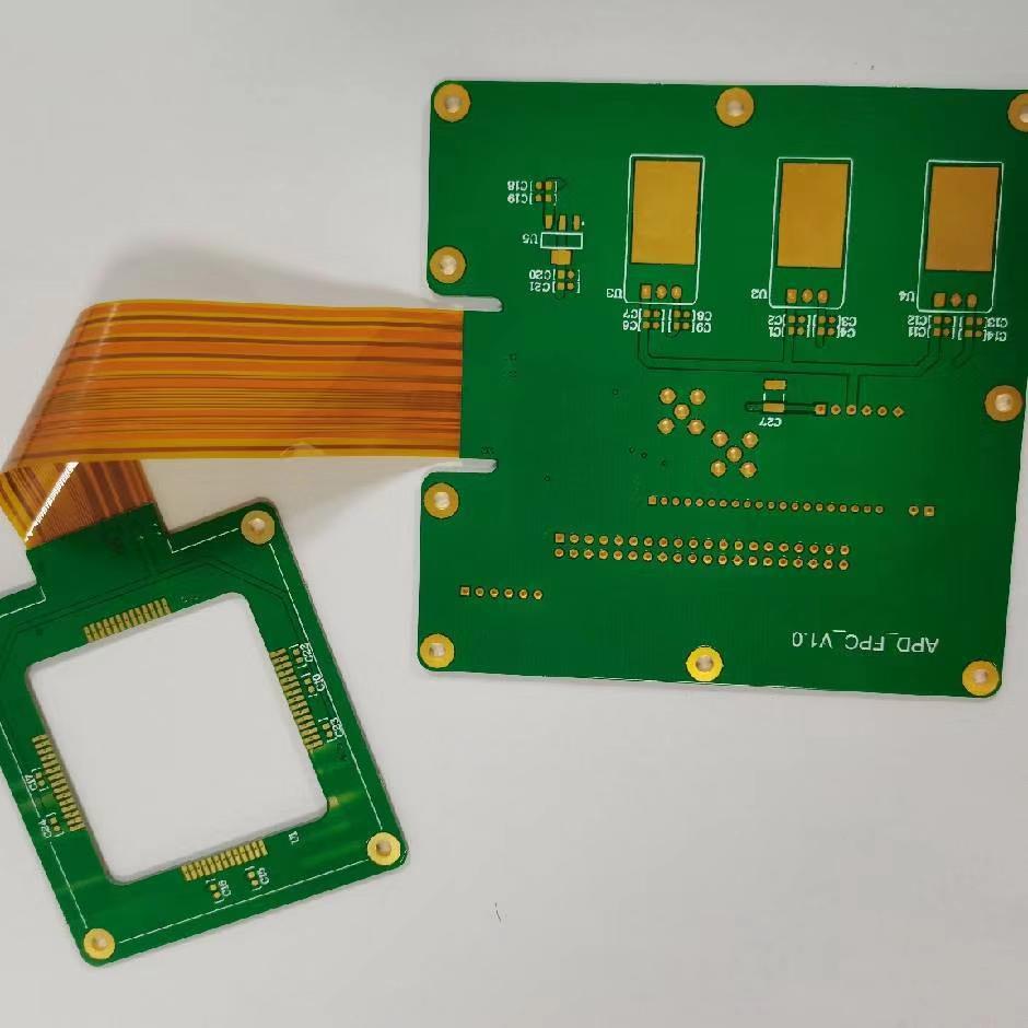
Fit Rigid Flex PCBs into an Enclosure
The enclosure's design is critical in determining how the product will function and feel. As with any product design, it should be created to fit the needs of its intended user. In the case of rigid flex PCBs, this means designing an enclosure that meets the functional requirements and one that fits well into the hands of consumers who will be using it daily.
One way is to use an adapter board to mount your printed circuit board onto another surface like a plastic enclosure or a larger piece of rigid material. Another option is to use a flexible enclosure that lets you bend the plastic around the edges of the printed circuit board to naturally fit inside the enclosure without any special tools or hardware needed.
The enclosure must be designed to fit the rigid flex PCBs, cables and other components inside it. If any of these components are not accounted for in the design process, then there is a chance that they will not fit well into the final enclosure. This can cause issues with assembly and manufacturing and poor performance once assembled.
Control and Maintain Flex Circuit Profile Tolerances
When creating a rigid flex PCB design, it is necessary to have control over the profile and thickness of the flex circuit. This requires that tolerance be set for each layer in the design. This ensures that the previous design can be used as a template when a new design is created. The following steps are used to set up tolerance parameters:
Step 1: Create an existing rigid-flex PCB design from which you want to use as a template.
Step 2: Open the new design in which you want to add flex circuits and set up parameters for the top copper layers first. Next, set up parameters for all other layers except those used by pads and vias.
Step 3: Select all copper layers except those used by pads and vias, right-click on one of them, and select Properties from the pop-up menu. The Properties dialogue box will open, showing all layers except those used by pads and vias. Set up tolerances for top copper layers only at this time since other layers will be added later after setting up parameters for them individually later on in this process.
Design to Maintain Rigid flex PCB Bend Radius Integrity
Bend radius is the maximum distance between two planes in a part or assembly that are parallel to each other and are separated by a particular radius. The bend radius is vital in designing the PCB because it affects the strength of the board and its ability to withstand stress.
Bend Radius Optimization
Designers need to keep the bend radius as small as possible while maintaining the electrical performance of the Rigid flex pcb board. They should also consider that it may be necessary to increase the thickness of specific layers or reduce the number of layers to maintain sufficient rigidity.
Bend Insensitive Technique
The bend does not affect most electronic components because they have been designed specifically for this purpose and tested for reliability with slight bends. However, some components may not be able to withstand an extreme amount of stress from bending, so designers should consider using the 'bend insensitive technique' to prevent these devices from failing when being bent during manufacturing or after installation into their final application.
Understand the Long-Term Reliability of Polyimide and Polyester Materials
It is essential to understand the long-term reliability of polyimide and polyester materials for the creation of rigid flex PCB Design. Polyimide and polyester are two of the most widely used materials for PCB manufacturing. Both materials have their advantages and disadvantages.
Polyimide is a thermosetting plastic material that is commonly used in electronics manufacturing. It is known for its excellent thermal stability, low dielectric constant, high breakdown voltage, and high dielectric strength. This makes it suitable for creating rigid flex pcb boards.
In comparison, polyester is a heat-resistant polymer with good mechanical properties and dimensional stability. This makes it ideal for creating rigid flex pcb boards with an embedded chip or other components that require high performance and durability.
Both polyimide and polyester have excellent long-term reliability when creating rigid flex pcb boards.
Ensure Mechanical Strength of a Rigid Flex PCB Assembly with Coverlay and Solder Mask
Rigid flex PCB design can be created using different materials, including FR4 glass epoxy laminate, thermoplastic polyimide (TPU), and FR4 glass epoxy laminate with TPU. The material you choose will depend on your application requirements, but it is crucial to ensure that your design has enough mechanical strength to withstand any force applied to it during use. To ensure the mechanical stability of your design, you should consider adding coverlay material over the top of the copper traces and solder mask treatment over top of all exposed copper areas.
Coverlay is a laminate film applied to the copper side of the rigid flex PCB and then covered with a solder mask. This creates an additional layer of protection around the components on the top side of the flex PCB. It can also help to reduce EMI (electromagnetic interference) by preventing any part from being exposed to open air.
The rigid flex pcb assembly process of applying coverlay involves adding solder paste to all the pads, placing them in a vacuum chamber, removing excess solder paste and applying a thin layer of adhesive to each pad. A film is then laminated onto each pad using heat and pressure. The result is an extra layer of protection surrounding your circuit board's components while keeping them accessible.
Final Word
While the industry is quickly progressing from a paper-based design methodology to one that relies more heavily on computer-aided tools, there are still many nuances to consider when designing a rigid flex PCB. Luckily, the new PCB technology benefits far outweigh any potential caveats. And with a bit of know-how and advanced technical knowledge from Hemeixin, you can rest assured your designs will come out looking amazing.


