How to Calculate the Flex PCB Bend Radius and the rigid flex pcb minimum bend radius?
Circuit boards have allowed humanity to step into the modern era. One can argue that they are the cornerstone of humanity's most recent achievements. All scientific research, whether concerning the life sciences or modern physics, requires complex electrical devices for accurate analyses.
Consequently, circuit boards provide the means to use electricity and breathe life into appliances and devices. Technology would merely cease to exist without them since they are virtually the foundation upon which all electrical products are built.
In recent times, they too have undergone quite some change. We now have printed circuit boards that aid us in developing increasingly intricate applications and systems. Printed circuit boards are divided into rigid boards, flex PCB boards, and rigid-flex PCB boards.
Perhaps, flex circuit boards can arguably be considered the most innovative of the three. In this article, we will explore their benefits, understand flex PCB bend radius, and finally teach you how to calculate flex PCB bend radius.
What is Flex PCB Boards
As the name suggests, this particular category concerns printed flexible circuit boards. These can be bent, flexed, or manipulated to fit inside an electrical design. The flexibility affords them greater versatility than traditional rigid circuit boards. Therefore, flex circuit boards are vital components in designs that require utilizing limited space.
As a result, their use has become increasingly popular in modern consumer electronics, smartwatches, information, and medical appliances. When correctly designed, they can be subjected to thousands of looping or bending cycles. It affords them uniqueness as well as a set of advantages over their rigid counterparts.
Flexibility
It goes without saying that flexibility is one of the biggest advantages of using flex circuit boards. This ability allows for more creative freedom and the ability to fit the circuitry into the design, limiting any creative compromises.
Reduced Weight
The circuit boards have to be very light and thin to achieve flexibility. This results in an overall reduction in weight which is an important factor in the modern world where lightweight products are preferred over heavier ones. The lightweight design of flex circuit boards also allows for increased flexibility and better shock absorption, which increases the long-term reliability of products.
Connectivity
Flex PCBs also increase the range of connectivity in a device and its electrical components. Their use in dynamic flex circuit applications is particularly popular since they require circuit boards that can be bent or flexed for an indefinite number of cycles. This makes them the top choice for use in foldable electronics.
Flex PCB Bend Radius
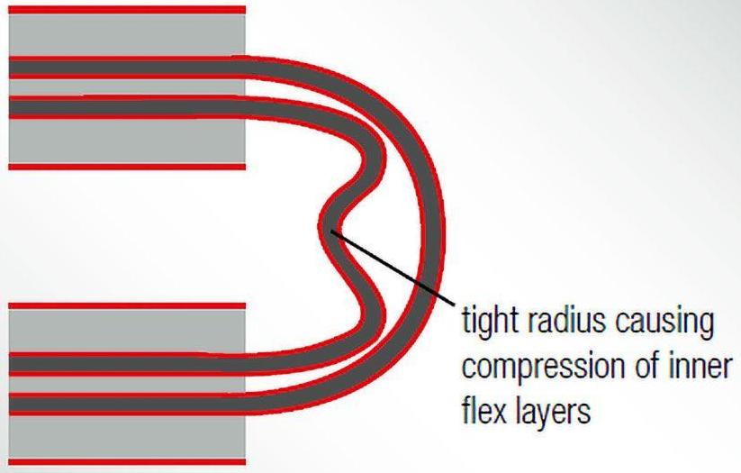
There is, however, a limit to the amount of strain flex PCBs can be subjected to. When they are bent out of shape, the internal bend experiences compressive forces while the external bend experiences tensile forces. Knowing the limits of these forces that the circuit board can withstand helps with the continued functionality and enhanced performance of an electrical device.
The bend radius is a measure of how much you can bend a flex circuit board without causing any damage or shortening its lifespan. The smaller the bending radius of a circuit is, the more flexible it will be. There are three types of design standards for flex PCB boards:
1. Flex to Install
This is also called the stable flex and involves the flex layer to be bent into shape to fit into a design. The bend is introduced in the beginning, and the layer is not subjected to further stress. For one or two layers, the minimum bend radius can be 6X, while for multiple layers, it can be up to 12X.
2. Dynamic Flex
This design involves repetitive bending of the design; therefore, limiting it to two layers is recommended. The copper should be allowed to sit on the neutral axis, which is the point that experiences minimal strain or stress. The minimum bending radius is roughly around 100X.
3. One Time Crease
Minimum bend radius is irrelevant in this design since the flex layer is creased before being installed into the design. Very thin layers and copper weights are recommended. The copper should be placed as near the neutral axis as possible.
How to Calculate Flex PCB Bend Radius
The minimum bending radius is calculated as a multiple of the final circuit board thickness and the ratio of the desired application (stable or dynamic) and bend radius (r):
Ratio = r/h; where r = bending radius, and;
h = overall height of the flexible part.
These are the bending radii for different layers of stable and dynamic flex boards according to IPC-2223:
| Layer | Stable | Dynamic |
| Single Layer | 10:1 | 100:1 |
| Double Layer | 10:1 | 150:1 |
| Multi-Layer | 20:1 | Not recommended |
To calculate the minimum bending radius of a single-layered dynamic flex circuit board with an assumed thickness of 90 µm, we will confirm the bending radius ratio from the table above and multiply it with the thickness of our application:
Min. bending radius = (r/h of single layer dynamic flex) x application thickness
= (100:1) x 90 µm (or 9 x 10⁻⁶)
= 9 x 10-4 = 0.9 mm
Therefore, the flex circuit board will have a resulting minimum bending radius of 0.9 millimeters. Similarly, you can calculate flex PCB bend radius for any application as long as you consult and tally accurate values from the abovementioned table. For more information on design guides for flex circuit boards, understanding the flex PCB bend radius, or for more innovative circuitry, visit Hemeixin Electronics.
Flex PCB Material Selection
Standard design practice is to minimize the thickness of the flex circuit as much as practical while meeting the electrical requirements of the design and not incurring unnecessary added material costs.
As a result the most common materials are as follows (in order of preference):
Copper Weight: ½oz , 1oz
Flex Core Thickness: 1 mil, 2 mil, 3 mil, 4 mil
Coverlay Thickness: 1 mil, ½ mil
Flex cores are also available in two different construction types: Adhesive and Adhesiveless, which based on the method used to attach the copper to the polyimide core.
Adhesive uses a layer of flexible adhesive to bond the copper to the polyimide core
Adhesiveless bonds the copper directly to the polyimide core
Radiused Corners within Flex PCB Bend Areas
Having a radiused corner within and flex bend area reduces / eliminates stress concentrators and improves reliability.
Staggered Layer to Layer Trace Positioning in your Flex pcb design
Staggering your designs layer to layer trace positioning eliminates the "I-Beam" effect which improves the flexibility and reliability of your flex PCB.
Cross-hatching plane layers to increase flex pcb flexibility
Use a cross-hatch or dot pattern to reduce the copper area on plane layers.
The amount of flexibility gained will be directly proportional to the percentage of copper removed from the plane. A cross hatched plane pattern can also increase bond strength between that layer and the adjacent layer since adhesives bond better to polyimide than to copper. This method should be used in cases where the plane functions primarily to control EMI. The percentage of copper that can be removed will depend on the frequency of the noise that the plane is functioning to keep out of the circuit. It should be noted that reducing the copper plane coverage will significantly impact the impedance of any signals using that plane as a return path. For this reason, it is advisable to look for alternate methods (such as silver epoxy planes) to increase circuit flexibility when impedance is a concern.
Cross-Hatching in Flex PCB and Rigid Flex PCB
While cross-hatching is rarely used in rigid PCBs these days, it does have practical application for both flex and rigid-flex PCB circuits. These applications come in two areas for flex and rigid-flex circuits:
- Controlled impedance in flex regions: Using a hatch ground is a good method for providing the reference plane required in controlled impedance routing for high speed digital boards. The hatch ground provides wider, more manufacturable dimensions while retaining the flexibility of the circuit and assembly. It should be noted that cross-hatching reduces the amount of copper under a transmission line, which decreases the capacitance and raises its impedance.
- Structural support for flex regions: Using a hatch ground provides structural support needed for a dynamic or static flex ribbon without increasing the rigidity of the copper layer. on a two-sided flexible circuit. The layer can still be used for controlled impedance routing creating undesired rigidity, or the ribbon can be permanently deformed.
In order to calculate a trace width that results in the correct impedance, it is necessary to use a modeling tool that accounts for the missing copper in the crosshatched plane. Because the impedance for a given trace over a hatch ground region is higher than that over a solid ground region, the inductance of the trace needs to be decreased to maintain controlled impedance. Therefore, we would want to make the trace a bit wider as this will reduce the trace's inductance and increase the total capacitance with respect to the hatch ground. Both effects will contribute to set the impedance to the correct value.
What do you have to know when rigid flex pcb fabrication?
1. Distance of plated holes (PTH) to flexible areas
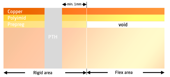
Plated drills (PTH) must have a distance of at least 1,0mm from adjecent flexible areas. The reason is that during chemical processing, a lot of fluuids are running through these drills. However, the flexibl area is hollow inside (not laminated). So the only thing keeping chemicals from flowing through the PTH drill and into the hollow part below the flex is this 1,0mm of laminated FR4-PI (in reality due to swelling drills and reducing the prepreg-flow, it is even less than that).
This graphic visualizes the challenge. The FR4 below the FPC will later be milled by z-axis depth milling, so that only the flexible part remains. But if chemicals flew into the hollow part underneath during production, the complete rigid-flexible board is scrap.
2. Traces in the rigid-to-flexible area
All traces coming from the flexible parts should run straight into the rigid area for a length of at least 1,0mm before bending or turning in other directions/angels. This is because in these transition areas the board encounters the highest mechanical strain. Diagonal traces or angels in this transition area create unnecessary sharp angels which tear easily.
3. Traces in flexible areas
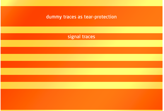
In order to maximize bendability of the flexible areas these traces should also run in straight lines. Angels or diagonally running traces may lead to an increased risk of tearing. If there is sufficient space we do recommend additional, thicker traces on to the outside of the flexible areas as a protection against tearing. These trace do not have to have an electrical function but can be inserted as "dummy" traces. However, these traces should also run at least 1,0mm into the rigid area.
Above graphic shows parallel running traces with thicker dummy traces on the sides. Of course you also decide to put an electrical signal on the outer traces.
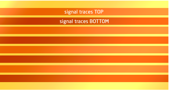
Regardless the stabilizing traces on the sides, for double-sided FPCs all traces should be aligned in a shifted manner so that they do not overlap. This reduces total flexible layer thickness and allows better bending performance.
Mechanical Requirements for Flex PCB and Rigid-flex PCB
Working with a flex PCB ribbon is all about ensuring components and traces on your board are not damaged under repeated bending. You’ll need to understand the mechanical properties of your materials to design the right bend radius, and many of the foundational concepts of rigid boards still apply. Although you want to prevent fracture, you also need to ensure your product will fit in its enclosure once the flexible ribbon is bent.
The ribbon in your rigid-flex PCB and flexible PCB circuit board will integrate directly into your layer stack as a signal layer and a pair of flexible surface layers. As you place additional features on a flexible design of a printed circuit board, you’ll need to model your board’s mechanical behavior. This allows you to check component clearances and match your board’s dimensions to your board enclosure.
Layer Stackup In Rigid-Flex PCB and Flex PCB
Your flex PCB circuits and rigid-flex PCB circuit boards will still have sections built up from common rigid PCB laminates. The most common rigid insulation material is called FR4. It is an industry designation that represents the ratio of fiber to resin, so materials may vary somewhat to meet FR4 resin content and glass weave requirements. For specialized applications, such as radio frequency or mmWave designs, other types of material designations are available. Consult IPC-2221 for listing of all PCB material types.
The ribbon in a flex or rigid-flex PCB is made from flexible polyimide, where traces are routed only in the internal flexible layers. The rigid PCB ends of the board are multilayer structures, and traces are routed across the flex ribbon between rigid sections. In some boards, the flexible circuit ribbon also has multiple layers, and a plane layer can be routed across a flex ribbon.
They are one of the leading manufacturers of flex circuit boards and Rigid flex PCB circuits, among other modern design models. They offer the best circuit boards to customers at affordable rates because you deserve the best solutions for your electrical designs! Take and look at their products and get a quote today!


