How to design rigid flex pcb - Hemeixin
What is Rigid-Flex PCB ?
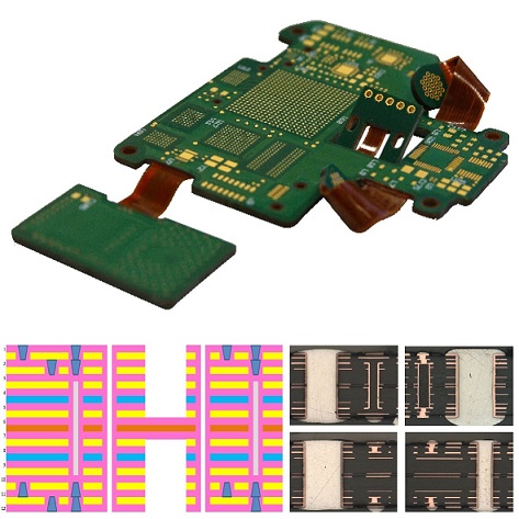
As the name suggests, a flexible printed circuit is a pattern of conductors printed onto a flexible insulating film. Rigid-flex PCB is the name given to a printed circuit that is a combination of both flexible circuit(s) and rigid circuit(s), as shown in the image.
Rigid-flex PCB design combines the best of both worlds – elements of standard “rigid” (usually FR-4) PCBs with flexible PCBs on a single board. These boards primarily consist of two or more rigid areas connected by flexible polyimide strips with copper cladding substrate. The board fabricator takes the rigid board and then adds through-holes to connect it to the flexible polyimide board.
Due to the complexity of rigid-flex boards, there is a lot that goes into their design. When you apply the design tips and methodologies that we’ll be discussing, you’ll be able to design rigid-flex boards that are reliable and able to withstand hundreds of flex cycles without failure.
Flexible circuit technology was initially developed for the space program to save space and weight. It is popular today as it not only saves space and weight - making it ideal for portable devices such as mobile phones and tablets - it can also reduce packaging complexity, improve product reliability, and reduce cost.
Flexible circuits are normally divided into two usage classes: static flexible circuits, and dynamic flexible circuits. Static flexible circuits (also referred to as use A), are those that undergo minimal flexing during assembly and service. Dynamic flexible circuits (also referred to as use B), are those that are designed for frequent flexing, such as a disk drive head, a printer head, or as part of the hinge in a laptop screen. This distinction is important as it affects both the material selection and the construction methodology. There are a number of layer stackup configurations that can be fabricated as rigid-flex, each with its own electrical, physical, and cost advantages.
What is Rigid flex PCB design?
Learn the specific applications of rigid-flex boards.
Where to place vias and route your rigid-flex board for reliable design.
Methods to set up an optimized stackup for rigid-flex board design.
Rigid-Flex PCB Design Basics
There is a lot that goes into rigid-flex PCB design. First, consider your application and the advantages and disadvantages previously mentioned. Once you’ve determined that a rigid-flex PCB design is the way to go, consider the board’s intended environment. Is the board meant for a dynamic bend or stable bend, and what is the bending radius?
A dynamic bend rigid-flex PCB is used in an environment where it will be constantly subjected to stresses and bending. In this case, use no more than two layers and ensure that the bending radius is at least 100 times that of the flexible material thickness. Once bent or flexed, a stable bend is meant to remain in that position. In this case, make sure the flexible substrate thickness is about one tenth the bend radius.
Envision your design in the three-dimensional environment it will operate in. A rigid-flex design is usually placed within an enclosure. Consider what mechanical forces and stresses the board may be subject to and ensure that the board within the enclosure is designed to deal with them.
Hole, Routing, and Fill Plane Guidelines for Rigid-Flex PCB Design
When designing rigid-flex boards, the area that is most delicate is the bend. For this reason, avoid placing pads, holes, and vias on these bending areas. Areas near the bending line can apply mechanical stresses that could tear or harm the structure of plated holes close to it. Keep your pads and vias on flexible areas that aren’t subjected to bending, or even better, on the rigid, hard section of the PCB.
If you are placing plated holes or vias on a flexible section, make sure you use anchors to strengthen them as well as a teardrop to connect to any traces. Keep these holes around 10 mils, with at least a 10mil annular ring around them. This larger size allows for easier anchoring and prevents peeling during flexion. In general, avoid placing holes, vias, or pads on flexible areas and place as many as you can on the rigid section. Try to keep them at least 15 mil away from the edge of the stackup, as there can be more instability towards the edge of the board.
Rigid flex PCB Layout guidelines
From the differences mentioned above, for the layout and use of rigid-flex printed circuits, the following can be deduced:
- For single-sided flexible circuits, the bending radius is approximately 6 x the thickness of the flexible material, and for double-sided circuits it is approx. 12 x the thickness.
- Choose track widths and spacing in the flexible region to be as large as possible (> 150 μm)
- The flexible region should have parallel tracks which are the same width, with the same leakage resistance, and which run at 90° to the bend line
- Tracks should extend at least 1 mm into the rigid region
- On flexible layers, include hatched copper areas which are as large as possible
- The tracks on double-sided, flexible parts should be symmetrically offset
- Holes should be at least 2 mm away from a flexible part
- Choose solder surfaces to be as large as possible, the diameter of solder eye pads should be at least twice the diameter of the hole.
- Solder must not come closer than 1 mm to the flexible area
- Add about 1 mm all round to the dimensions of openings in non photostructured covering films
- To be able to assemble the components on a board, to solder & check them, a stiff frame with defined breaking points should be used. Blanks can contain single or multiple
boards. - Always use smooth (round) milling transitions to the connected parts of the circuit
Routing for Rigid-Flex PCB Boards
In regard to your traces and routing, keep your traces as straight, perpendicular lines. If your board bends or folds along a horizontal line, then have your traces run vertically. Traces should ideally go in one direction, but in the case where changing directions is a must, curve the traces as opposed to sharp 45 or 90 degree corners. This will eliminate high-stress areas from your board. Use narrower traces that are evenly spread out across a flexible area to decrease areas of high stress. Adding in dummy traces or even redundant traces can help increase the mechanical sturdiness of the flexible areas and protect traces from breaking the signal path completely. In the case of traces on both the top and bottom of a flexible section, alternate them such that a bottom layer trace has no top-layer traces immediately above it, and a top layer trace has no bottom- layer traces immediately below it.
For your power, signal, and ground planes, if you pour a typical plane with a solid area of copper, you’ll end up putting a significantly large amount of stress on your board and reduce its flexibility. Instead, use a hatched-polygon pattern for the plane. Minimize your trace widths on the fill as well, but be aware that a cross-hatch isn’t great for high-speed signal integrity.
1. Rigid-flex transition
Just like the broken headphones, the most vulnerable location is always the transition between flexible cable and rigid insertion end. The transition between rigid and flex circuit board is also the area for careful design. The rule-of-thumb for conductor spacing is 5 mm between the rigid board and the bend area of the flex circuit. Conductors closer than this are much more susceptible to breakage. Also, without proper spacing, the coverlay under the rigid area can peel and expose copper.
2. Minimum bend radius requirement
One successful practice to design a flex design is considering the bend requirements. Both the material type and thickness will impact the bend capability of the flex session. The minimum bend radius is usually calculated by using the flex thickness multiply a factor. Bend to fit applications use a factor from 6 to 20 depending on the layer count. Dynamic bend application is typically using 100 multiply the thickness of a 1-2 layers flex design.
3. Conductor width
Conductor width is also especially important. A safe rule-of-thumb for conductor widths is to design them at least five times as wide as they are thick. Our recommended practice is to use the thinnest copper trace that will safely carry the intended signal and then adjust trace width accordingly. For example, if a signal can perform as required on ½ oz. copper, the trace width should no less than 3mil.
4. Air gap in rigid-flex
For multiple layer flex design, it is better to configure the flex layers in independent pairs, instead of designing all flex layers together. This configuration is known as “air gap” or “loose leaf design”, with an air gap designed between each of the flex layer pairs. Another benefit of the construction with air gap is that it can significantly increase the flexibility of the design.
5. Thermal expansion
Most adhesive-based flex base materials are unfilled, which may result in unchecked thermal z-axis expansion, which makes vias and other features prone to delamination and causes potential intermittent responses after components have been soldered to the surface of the flex material. To combat this, include a more robust pad stack compared to the rigid areas for components soldered on the flex material. Rigid-flex circuit designs are increasingly popular with the miniaturization of technology and the explosion of wearable devices. Rigid-flex circuits require unique manufacturing processes and thus have unique manufacturing process constraints.
Rigid-Flex PCB Board Design Standards
There are numerous standards for rigid-flex boards that are worth consulting. IPC 2223, for example, specifies coverlay construction, adhesive flex cores, air gaps, strain relief filets, and pre-bake requirements for your board. Additionally, it includes tips for the location of plated vias or holes near the transition region from rigid to flex.
This area is unique in that the polyimide coverlay which encapsulates the flexible areas must overlap with the rigid areas by a small distance to ensure they are encapsulated by the rigid area of the lamination process. The coverlays are attached to the flex surface with adhesive made out of acrylic or epoxy. If vias are drilled through the adhesive, they can be subject to stresses from the adhesive expanding or contracting due to the high thermal coefficient of expansion, especially during reflow temperatures. IPC 2223 specifies a minimum distance of 0.125”, but many manufacturers can deal with smaller keepout distances.
Stackup and Board Design for Quality Rigid-Flex PCB Boards
When deciding on materials for your rigid-flex board, it’s important to communicate with manufacturers to ensure proper flex behavior. Specifically, pay attention to various mask types, dielectrics, stiffeners, and thickness of copper layers, as these can impact your board’s ability to bend. Make sure to also pay attention to the flammability rating, mechanical considerations, and impedance control for each board.
Broadly speaking, a rigid flex design will closely resemble a hardboard design, with the flexible layers fully extending into the rigid areas of the board. Similarly to hardboard layouts, a rigid flex fabrication package will include Gerber layers, along with drill files, solder mask layers, nomenclature, perimeter/rout files, coverlayer, etc.
However, there are some key differences between the fabrication packages for rigid flex PCB’s and hardboard applications:
- A rigid flex print generally has many more dimensions on it, and should carefully define the requirements, as these boards are generally used in 3D applications. It should also accurately define the rigid to flex transition areas, as these are not always apparent when viewing the Gerber layers alone.
- The material layup in rigid flex boards is critical, and should be worked out in collaboration with your fabricator. Your fabricator can help you make the right choices in materials based your requirements such as UL flammability rating, minimum bend radii required, mechanical considerations, impedance control on both flex and rigid layers, RoHS certification, lead free assembly compatibility, and other considerations.
- Rigid flex boards usually require additional layers in the Gerber files. Layers 1 and X will have solder mask layers, but you will also need artwork layers that define the coverlayer and bondply sections (if required) of the board, and how much each go into the hardboards. IPC 2223 recommends 0.100″ but your fabricator may be able to accommodate less than that.
The IPC-2223 Sectional Design Standard for Flexible Printed Boards is an excellent resource for wise practices in both flexible circuit and rigid flex PCB design.
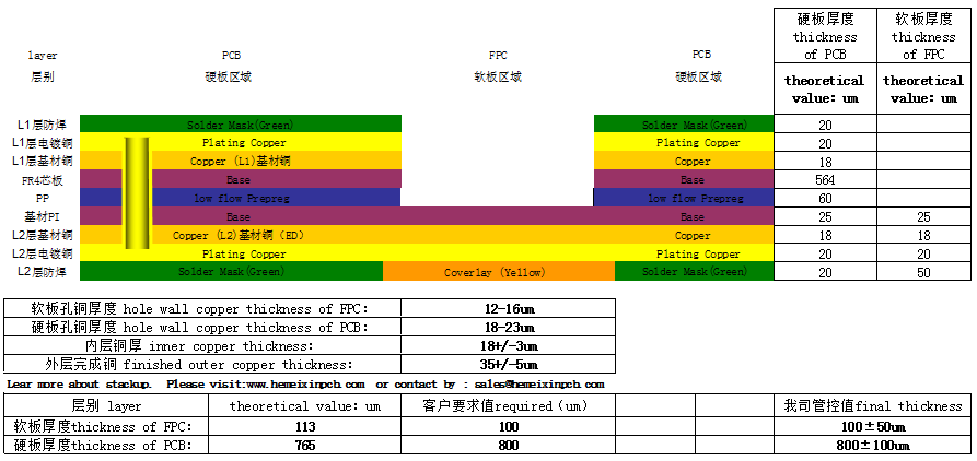
Common 2 layers rigid flex pcb Layer Stackup
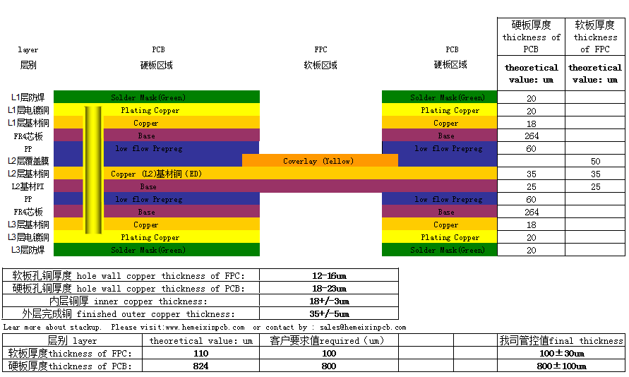
Common 3 layers rigid flex pcb Layer Stackup
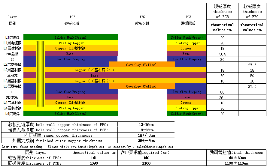
Common 4 layers rigid flex pcb Layer Stackup
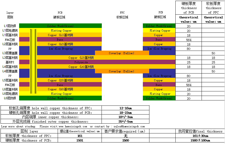
Common 6 layers rigid flex pcb Layer Stackup
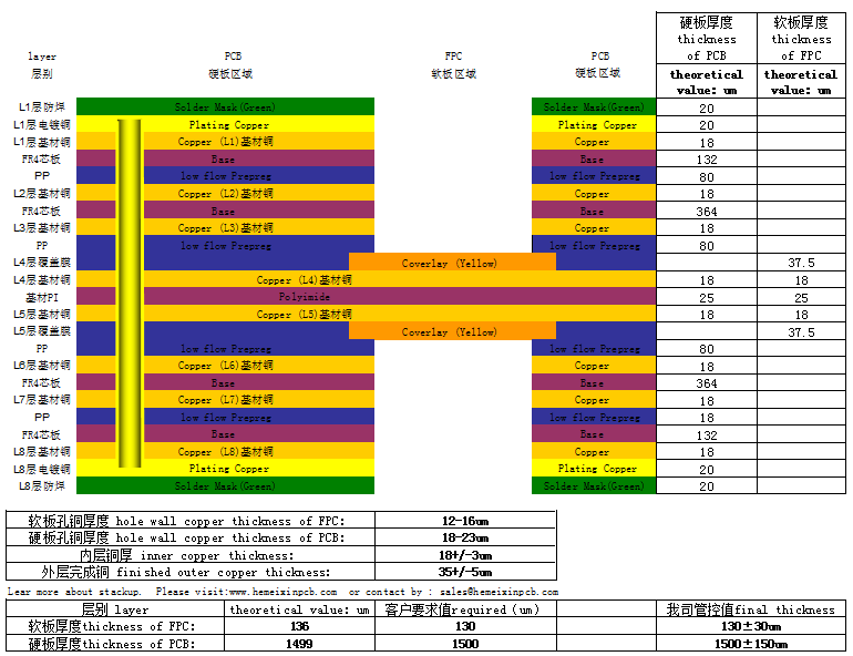
Common 8 layers rigid flex pcb Layer Stackup
Flex and/or rigid flex printed circuit boards typically contain copper, polyimide film and an adhesive material which are all laminated or bonded together through heat and pressure. The copper that is used comes in the form of foil for greater flexibility. Polyimide film is the non-conductive layer that surrounds the copper – it is flexible, but extremely reliable, so it is able to withstand the heat and pressure of the lamination process as well as the environment of the final end-use application. Finally, the adhesive layer is used to bond the layers together. Although acrylic is typically used as the adhesive, it may pose manufacturing problems for certain designs including squeezing into copper areas to cause electrical problems, and moisture out gassing to cause delamination or debonding. Because of this, non-acrylic and adhesiveless options are available as well. Your manufacturer will be able to advise you on the best form of bonding to use for your stack up as well as other material suggestions to avoid problems.
See also: Rigid flex PCB design guidelines
Using the correct materials and thickness of materials is crucial during the lamination process. An incorrect stack up could cause defects, delamination and in some cases, can even cause the part to explode. Your manufacturer will have different choices for materials as well as thickness, and can recommend the best options for your design. Be sure to work with your manufacturer early on in the design process to make sure your materials and stack up are ready for lamination.
Rigid flex PCB Minimum bend radius capabilities
Assuring the flex board meets the bend criteria is important for a successful design. A flex section’s bend capability is determined by the materials and the thicknesses utilized. Minimum bend recommendations are provided by IPC 2223 standards for both static and dynamic applications. The minimum bend radius is determined by the flex thickness multiplied by a factor that depends on the layer count. The tables below define the bend requirements for static and dynamic applications.
Bend requirements for static applications
| Number of layers | Minimum bend radius |
| 1 to 2 | 6 times the flex thickness |
| 3 or more layers | 12 times the flex thickness or more |
Bend requirements for dynamic applications
| Number of layers | Minimum bend radius |
| Limited to 1 or 2 layers | 100 times the flex thickness |
IPC 2223 also allows a flex section to be bent and creased with a zero bend radius if certain standards are followed. This is limited to very thin one and two layer constructions, with the additional restriction that the flex cannot be unfolded once it has been creased. In the fold area, a PSA (pressure-sensitive adhesive), is frequently used to firmly affix the flex and prevent it from being accidentally unfolded.
Rigid Flex PCB Materials
Cover/substrate: Polyimide film: ½ mil (12μm), 1 mil(25μm), 2 mil (50μm), 3 mil (75μm), 4 mil (100μm), 5 mil (125μm); LiquidPhotoimageable Coverlay (LPI); Epoxy glass or polyimide glass (rigid-flex).
Conductor: Copper: 1/8 oz. (5μm), 1/4 oz. (9μm), 1/3 oz.(12μm), 1/2 oz. (18μm), 1 oz. (35μm), 2 oz. (71μm), 3 oz. (107μm)
Cupronickel: 0.625 mil (15μm), 0.9 mil (22μm), 1.3 mil (33μm),1.9 mil (48μm), 2.3 mil (58μm)
Nickel: 2 mil (50μm), 5 mil (125μm)
Adhesive: Acrylic, flame retardant acrylic, epoxy, epoxy prepreg, polyimide prepreg.
Stiffener: Epoxy-glass (FR-4), polyimide-glass, polyimide, copper, aluminum
Flex PCB base material:
Flex PCB base material consists of a foil made of flexible polyester or polyimide with tracks on one or both sides. Hemeixin uses polyimide materials exclusively. Depending on the application, we may use Pyralux® and Nikaflex® made by DuPont®, the glueless flexible laminates in the Felios®Flex series made by Panasonic.
Apart from the thickness of the polyimide, the materials mainly differ in their adhesive systems (on glueless, epoxy or acrylic basis) as well as in the copper quality. For comparatively static bending applications with a low number of bend cycles (for assembly or maintenance) ED (electro-deposited) material is adequate. For more dynamic, flexible applications RA (rolled annealed) materials must be used.
Materials are selected on the basis of the product and production specific requirements, and the datasheets of the materials used can be requested as required.
Flex PCB Adhesive systems:
As a bonding agent between the flex and the rigid materials, systems using adhesive on an epoxy or acrylic basis (which is still capable of reacting) are used. The options are as follows:
- Composite film (polyimide film coated on both sides with adhesive)
- Adhesive films (adhesive systems poured onto a paper base and covered with a protective film)
- No-flow prepregs (glass mat/epoxy resin prepreg with very low resin flow)
Hemeixin mostly uses no-flow prepregs as bonding agents.
The characteristics of flex materials
Flex materials differ from rigid materials in their essential characteristics, which have to be taken into account:
- Significant reduction of copper adhesion at higher temperatures (e.g. when soldering)
- Increased water absorption
- Changes of dimensions which are larger, by a factor of up to 10 in the individual production stages, especially for wet processes
Rigid flex PCB Strain relief fillets
A strain relief fillet is a flex bead made of epoxy. These fillets are gen erally applied to the rigid-flex transition zones. Fillets enable the flex to bend gradually rather than being bent tightly.
Implementation of fillets reduces the chances of damage in the copper circuitry around the transition zone.
IPC 2223 specifies a minimum 0.010" vertical spacing between the rigid section and the flex layers. This ensures optimum spacing for the bead to prevent it from reaching the adjacent rigid section. The fabrication drawing specifies the strain relief needs.
Rigid flex PCB assembly Processing notes
In principle rigid-flex printed circuits can be soldered without restrictions using the parameters for rigid printed circuits.
As polyimide film is however very hygroscopic, it is vital to dry it before soldering. If this is not done, delamination may occur, bubbles may form or sleeves may rip out during the soldering process.
We recommend drying for >4 h at 120°C and then processing immediately (<8 h) afterwards.
When designing rigid-flex printed circuits, there are many possible options for the construction and for the materials used. Please get in touch. Together, we can produce the ideal solution!
Conclusion
Rigid flex PCB material layups heavily influence cost, manufacturability, and final PCB performance, so it’s essential to spend time determining the ideal material set. For instance, controlled impedance, resistance, and current-carrying requirements are all important considerations that affect both copper weights and material selection.
A PCB designer should collaborate with their board fabricator to discuss these variables, so that the resulting design complies with all signal integrity requirements. Once the designer has performed initial calculations, the fabricator can verify them, and provide a more accurate modeling of the impedance characteristics of the board, and material set required to achieve those values.
The rigid sections of rigid flex boards are usually 20 layers or less. There are times when they have more, but usually more than twenty layers is pretty rare. The hard board sections don’t all have to have the same layer count. For example, you could have one rigid section with 16 layers of circuitry and one with 12. As long as the material layup is similar for each and the boards have the same overall thickness, there will be no manufacturing issues. Occasionally, a design may use hardboards that differ in thickness, but such configurations are substantially more difficult to manufacture, and other options should be considered.
See also:How to Reduce Rigid Flex PCB Costs
The flexible sections of rigid flex boards are usually one (singlet), two (doublet), three (triplet) or four layers (quad construction). There are times when a designer needs more than four layers across the flexible sections of the board, but are almost always unbonded. Bonded flex sections that have more than four layers can be very resistant to bending and or flexing. Copper weights on the flexible layers of the rigid flex boards are most commonly half and one-ounce weights. Occasionally the electrical demand requires two-ounce weights. In those instances, the designer should work very closely with their fabricator to choose the correct no flow prepreg, to adequately fill the thicker circuits in the hardboards. No flow prepreg, by design, does not like to flow and two-ounce circuitry can present some challenges. Three-ounce copper weight is rarely used, and can present substantial issues in manufacturing for the same reason.
Here we’ve provided an overview of rigid flex PCB design considerations and how to ensure that your design will be successful.
At Hemeixin, we manufacture rigid flex PCB circuits based on your exact specifications, and we aim to provide all the resources you need to help you optimize your PCB as early in the process as possible. To learn more about rigid flex PCB designs or about our capabilities and services, contact the Hemeixin team today.
