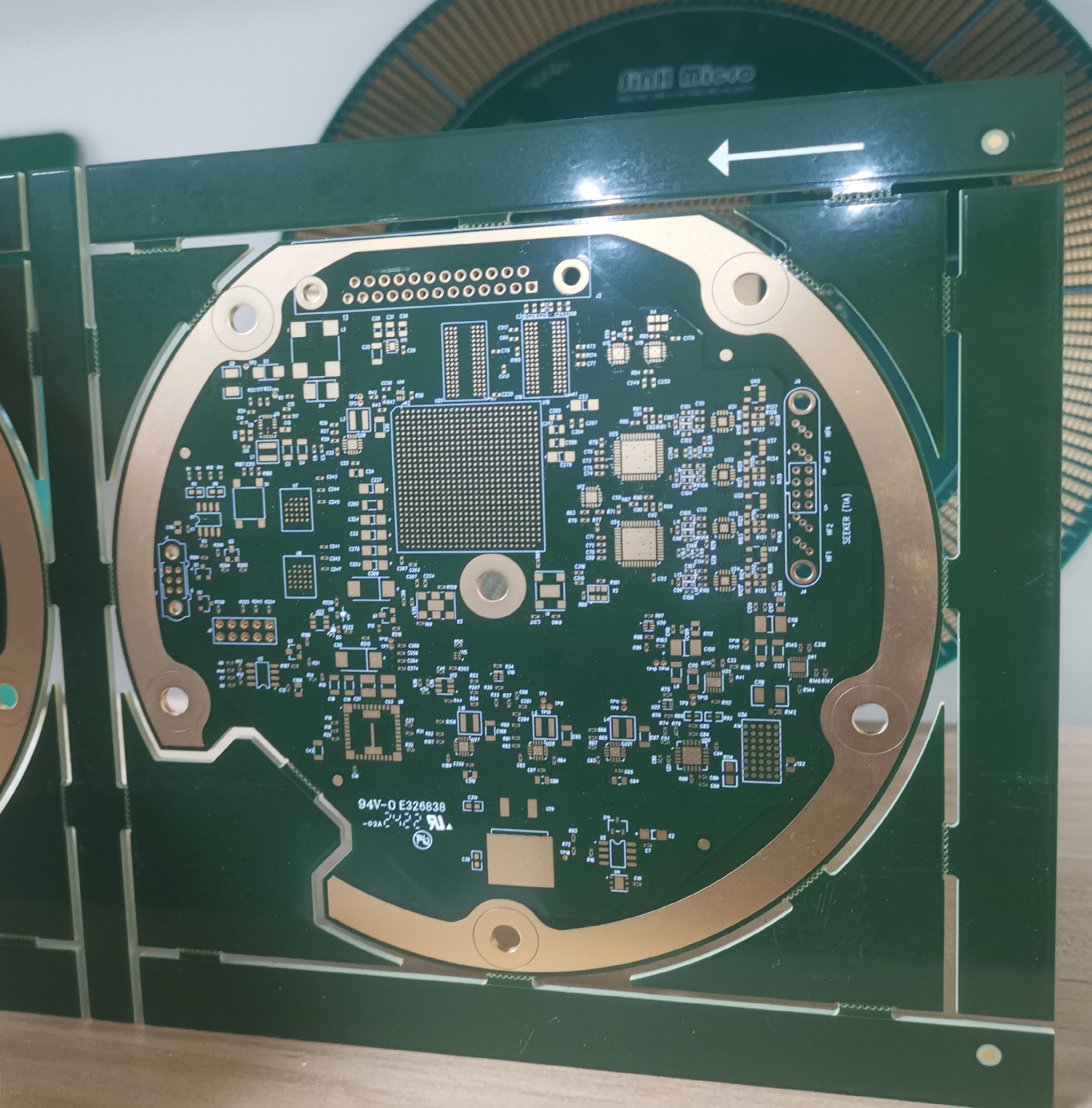
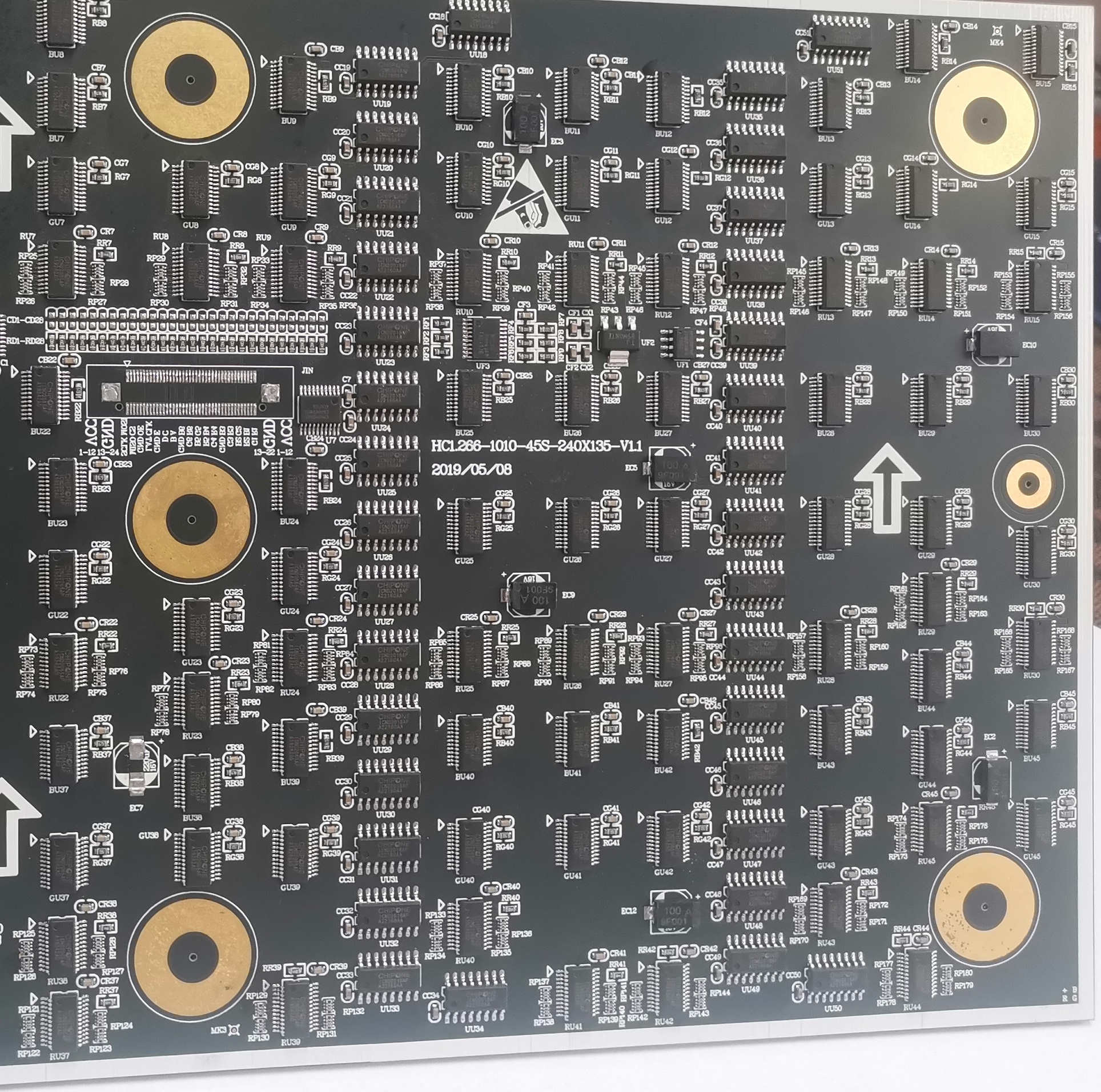
ELIC PCB and HDI Multilayer Designing
The world of electronics is getting increasingly complicated with new features and functionalities being introduced nearly every day. At the same time, electronic devices are getting smaller as manufacturers pursue miniature technologies. This brings us to ELIC in HDI PCB design.
ELIC, also known as every layer interconnect, is one of the most complicated HDI routing and stack up design styles used today.
It is based on a simple premise: to distribute microvias throughout the HDI PCB stackup to route signals on HDI PCBs between layers within the board. They are built one layer at a time using drilling, playing, etching, and pressing layers to a base layer set.
ELIC comes with certain restrictions and can overwhelm the fabrication process. It also puts a constraint on the materials used to design the boards.
Designing with ELIC PCB
Some designers may refer to ELIC as every-layer HDI. In other words, it is a reference to routing signals between any layer within the stackup on high density interconnects.
These circuit boards may contain several layers of microvias to facilitate even more complicated high density interconnections. When designing with ELIC, every layer has its own laser-drilled microvias that are filled with copper.
It is important to note that ELIC only makes use of copper filled stacked microvias to establish connections between layers. This makes it easy to connect two layers in the board after stacking them.
This process increases the board’s level of flexibility and allows you to maximize the interconnect density of the board.
A major advantage of designing with ELIC is that it makes through-hole vias redundant. This is because all connections within the HDI PCB are already created. Furthermore, you don’t need to use playing techniques to fill vias (such as VIPPO) because ELIC uses a copper filled structure.
Since we have stacked microvias distributed throughout the stackup, it goes against IPC warnings about microvia reliability.
ELIC microvia PCBs are not without their disadvantages. For one, they are highly vulnerable to latent defects from reflowing applications. Make sure to only choose a reliable manufacturer to ensure that your board passes quality tests.
A Close Look at The PCB Manufacturing Process
ELIC PCB manufacturing starts using a very thin core that comes with a solid copper-filled base and laser-drilled microvias.
Dielectric layers are added in a sequential lamination once the initial microvias on the inner layer are filled with copper. The new layer is subjected to laser drilling to build the ELIC micro via PCB stackup.
This is followed by filling the microvias in the new layer with copper. The process is repeated until the designer stack is built with the help of copper filled microvias.
The end result is improved durability and reliability of the HDI PCB. Furthermore, the copper fill goes a long way in preventing the dimping or voiding of the interior microvias.
Tips for Designing with ELIC PCBs
There are a few things you should know when designing with ELIC PCBs, in addition to the recommendations that your fabricator provided you. Here are a few tips to consider:
- Specify filled microvias in the inner layer to avoid dimpling and voiding.
- Select the right microvia aspect ratio to increase the reliability of the board.
- Maintain symmetry of the layers throughout the PCB board.
- Make sure to account for trace width and when pairing up layer thickness to achieve the desired impedance. This will help you work on your fanout strategy.
Major Applications of ELIC PCB
ELIC PCBs are primarily found in memory cards and graphic processing units. They are increasingly found in consumer gadgets such as wearables, tablets, smartphones, and other devices. These applications often require electronic components with a fine pitch and high pin count.
The HDI PCBs also use 5 or more layers. ELIC is a great way of achieving device miniaturization because designers can route interconnects within the PCB without requiring more real estate.
ELIC PCBs are mostly used in high speed circuits such as FPGAs that utilize multiple interfaces within the device. ELIC is also used in boards to support RF PCB routing on polytetrafluoroethylene materials.
A major concern for designers is impedance mismatch that could result in return loss. It is possible to circumvent this problem by routing across layers without leaving stubs in the PCB without having to back-drill.
It is worth noting that dielectric losses across these layers will be more pronounced as the routes get longer.
ELIC design may also be used with rigid-flex PCBs. They make it possible to reduce package sizes by using ELIC PCBs with rigid-flex PCBs in a single stack up. It is important to work with a bend region to prevent stress on microvias.
A major advantage of using ELIC is that it also allows the use of ribbons with smaller boards.
Single layers in high speed, high density designs will feature multiple ground and power planes to shield signal layers and minimize cross talking. This allows the device to comply with EMC by keeping excess radiation at bay. Higher layer count stackup can also provide support for high density fanouts while also complying with EMC.
Doing so will require the designer to implement creative strategies of the layouts to keep the signal layer count as low as possible while maximizing the use of real estate. This can reduce both EMI and crosstalk.
The high density wiring and degree of freedom makes these PCBs ideal for use with smaller devices such as smartphones and various high performance devices. In the years to come, ELIC PCBs will play a vital role in the miniaturization of technology.
Wrapping Up
ELIC PCBs are a technological feat that improves electrical connections between inner layers. The biggest advantage of using the technologies is that all layers within the circuit can be freely interconnected.
ELIC PCBs span a wide range of industries including military, automotive, industrial, telecom, and consumer electronics.
Hemeixin PCB is a leading quickturn HDI PCB manufacturer that specializes in high-tech industries around the world. They are a one-stop shop for all your PCB needs. For more information about designing with ELIC PCBs, get in touch with the experts at Hemeixin PCB.


