Factors That Impact RF PCB Design
RF PCB design is a vast field that covers not only many topics but also the design of systems, the selection of components, and the implementation of the whole circuit. A well-designed high-performance RF PCB is indispensable for any electronics system and determines its success or failure in the market. RF designers are responsible for various tasks, from simulations and calculations to creating their designs' physical layout. Considering that such designs are constantly evolving, it is imperative to grasp how you can optimize your approach to ease the entire process.
There are a lot of factors that will impact RF PCB design. This blog post will give key pointers about some considerations and factors that might impact your design strategy. Achieving balance in all of these aspects is crucial in RF circuit design, so it will work flawlessly and produce a functional and cost-effective PCB that meets your requirements.
Designing RF PCBs – Factors That Impact Design
Board Material
The material used in constructing the radio-frequency printed circuit board is an essential factor that impacts the performance of the RF PCB design. The most popular materials used in making RF PCBs are FR4, Rogers, Taconic, and other similar materials. These are generally used for high-frequency applications as they have high dielectric constant values. This makes them perfect for use in microwave applications where high frequencies are involved.
The thickness and type of material used in making an RF PCB can also impact its overall performance. For example, if you use a thick material, it will take more time to manufacture and cost more money than a thin one. However, using a thin material means that there will be less material between coils, which may result in interference when working at high frequencies.
Impedance Matching
For high-frequency operation, impedance matching is essential for ensuring proper working conditions for any circuit. A circuit works efficiently if its input impedance matches its output impedance at all frequencies. If there is a mismatch in impedance level, energy dissipates as heat instead of being transferred efficiently from one point to another. Therefore it is essential to match the impedance levels appropriately between different parts on the board, such as power supply connections and antenna connections.
For example, if two components have different impedances or reactances, they will not be able to send or receive signals effectively because of the mismatch between them. You can use resistors or capacitors to match the impedances of each component so they work together smoothly without significantly affecting each other's performance.
RF Ground Plane Design
The ground plane is an integral part of the RF circuit board as it helps reduce the overall size of the board and also helps in improving its performance. This ground plane can be made from different materials, but it is better if it is made from copper as it has good conductivity, which helps in increasing efficiency and reducing losses. It also helps improve heat dissipation by providing thermal and electrical paths for heat flow away from components like transistors or amplifiers.
RF PCB Stack-Up
RF PCB stack-up refers to the arrangement of different layers in an RF board. These layers may be conductive or insulating and are used to form electrical pathways between different sections of a circuit. These pathways enable current flow through the circuit, allowing electronic components (chips) to perform their intended functions. The thickness and composition of each layer impact how well signals travel through them and how efficiently they dissipate heat.
RF PCB stack-up consists of several layers: ground plane, signal, and power planes. A good stack-up should provide sheet resistance and effective shielding for the desired frequency range. It is also vital to consider each layer's dielectric constant and loss tangent, the thermal conductivity of each layer, and board thickness for different frequencies.
Power Dissipation
The power dissipation is a significant factor when designing an RF board. The high-power transmitters and receivers require special attention to ensure they do not overheat or burn out. You must consider the maximum allowable power dissipation of the components and use proper thermal management techniques such as heat sinks, fans, and heat sinks to ensure good cooling. In addition, you should also ensure that there is sufficient space between components, so they do not generate too much heat near each other.
Power Amplifiers
While power amplifiers are not directly related to RF PCB design, they can significantly impact the quality of your finished product. Power amplifiers amplify signals transmitted over long distances or through thick walls or other obstructions. The higher the quality of your power amplifier, the greater the distance you can transmit signals with minimal interference or distortion. You should always use high-quality power amplifiers in high-frequency applications where signal quality is critical.
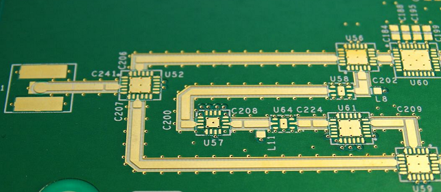
RF Trace Design
The layout of the traces and the spacing between them are critical to the performance of your product. If you have too many close together, you can get cross-talk. If there is too much space, it will take longer for signals to go from one part of the circuit to another.
Therefore, the traces for RF circuits must be designed with a specific set of parameters in mind. First, they must be wide enough to handle the signal without loss or distortion. The second is that they must be thin enough so as not to cause impedance mismatches that affect frequency response or cause reflections and interference. The third is that they must be adequately terminated, usually by an impedance matching device at either end of the circuit path, so there are no reflections or other problems due to impedance mismatches.
Via Design
The size, shape, and placement of vias on a PCB can significantly impact electrical performance. Via Design is a critical factor in determining the impedance of a trace.
Via Hole Diameter
The larger the diameter of the via hole, the lower the trace impedance. This is due to increased copper fill that results in more metal area between two planes to carry current.
Via Hole Depth
The greater the depth of a via hole, the higher its impedance because it increases the capacitance between two planes. A shallower via would have less capacitance but is more susceptible to cracking during reflow soldering. When selecting an optimal via depth, it is essential to consider how much current your circuit will draw and how robust it needs to be against thermal expansion and strain.
Via Spacing
Increasing spacing between vias will reduce their impedance because there will be fewer vias per unit area compared with densely packed vias in close proximity.
Power Supply Decoupling
Power supplies are one of the most critical components in any RF system. They can be prone to high noise levels and electromagnetic interference, which can cause damage to other components. Decoupling capacitors are used to reduce this effect. Decoupling should be placed near the power supply, as close as possible to the connected ICs. The best position for a decoupling capacitor is between the power supply and ground plane, where there is no circuit trace or signal path that could cause cross-talk.
There are two types of decoupling capacitors: X capacitor and Y capacitor.
X Capacitor
This capacitor is designed to be placed on a single-sided board to reduce high-frequency noise from VCC or ground pins. The X capacitors are usually made from polystyrene or polypropylene film and have a low ESR. They are usually placed near high-speed digital lines, clock signals, power lines, etc., to reduce high-frequency noise coming from these areas.
Y Capacitor
The Y capacitors reduce ripple voltage on the output of DC/DC converters or battery supplies. These caps should be placed close, such as 1", to the source output pin to reduce ripple voltage on that line.
Antenna Size
The size of your antenna will directly impact your signal strength and range. For example, larger antennas have more surface area than smaller ones to pick up more signals. If you want to improve signal strength, consider increasing the size of your antenna.
However, it is essential to consider how much space is available in your device before making any changes. If there is not enough room for a larger antenna, there may be other ways to improve performance without sacrificing space or aesthetics — such as using multiple smaller antennas instead of one large one or using a different material, for example, copper instead of aluminum.
The Bottom Line
RF and antenna design require multiple considerations throughout the product development process. They involve an expert and holistic knowledge to ensure that the proper design is implemented through production. With this information, a designer can ensure that the finished product meets their performance requirements and satisfies any other constraints.
Moreover, having a reliable PCB fabrication, assembly, and test partner will make all the difference when optimizing your product's performance. If you are looking for a reliable RF PCB manufacturer, check out Hemeixin.


