PCB manufacturing process steps have great potential for development in the future
PCB manufacturing process steps have great potential for development in the future, because PCB's form is diverse, so PCB manufacturing process steps It is also varied.
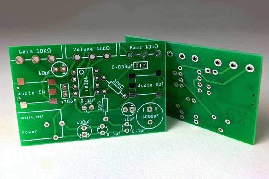
PCB has single-sided PCB, double-sided PCB, and multi-layer PCB, but even if it is a single-sided structure, the material and shape of the cover film and the reinforcing plate are different, the process of PCB manufacturing process steps will change greatly, so Even a single-sided PCB that looks simple, it's PCB manufacturing process steps The basic program is not simple.
Due to PCB manufacturing process steps Variety, the following example illustrates a PCB manufacturing process steps:
- 1. Making a traditional FPC;
- 2. Obtaining a solid FPC;
- 3. Baking the material, drying the resin in a 120-degree hopper for 4 hours;
- 4. Opening the mold by the injection molding machine;
- 5. Sol;
- 6. Clamping;
- 7. Injection;
- 8. Cooling;
- 9. Finished fit;
- 10. Bending;
- 11. Inspection;
- 12. Finished packaging.
With the wide application of PCB, almost every electronic device, from electronic watches and calculators to computers, communication electronic devices, and military weapon systems, must use PCB as long as there are electronic components such as integrated circuits.
Therefore, the innovation and improvement of PCB manufacturing process steps is extremely important, so it is important to explore a PCB manufacturing process steps that are easier to operate, reduce costs and improve performance.


