Explain like I’m a Designer: ELIC PCB and HDI Multilayer Designing
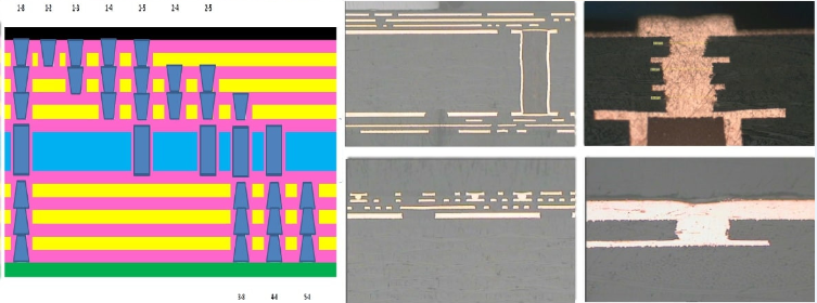
In the electronics industry, PCBs have been the de-facto medium for avionics and sensor development for a long time. Multilayer PCB stackup has been used extensively for connectors, accessing components (vertical interconnect), analog and RF designs, and heterogeneous integration of CMOS and BiCMOS in complex applications such as power converters. As new PCB technology becomes available, so does multilayer design complexity. A multilayer PCB has several layers to perform diverse functions, where multi-pair wires are used for interconnections between different functional layers or modules.
One of the most complex PCB design technologies is multilayer using Every Layer Interconnect (ELIC) and High-Density Interconnect (HDI) technologies. The following article walks you through the ELIC PCB and HDI multilayer design.
What is an ELIC PCB?
Every Layer Interconnect (ELIC) refers to a PCB design where all signal layers and the internal ground plane of the board are aligned in such a way that direct component and signal routing between two points in the design can be made without requiring a connection to be routed through one or more additional mechanical layers.
ELIC implements an enhanced version of the HDMI standard. It uses the same cable connectors and supports the same video resolutions as existing HDMI devices. The only difference is that you can transmit data at much higher speeds than possible with HDMI.
The ELIC protocol allows for data transfer rates up to 10GB/s per lane, which is about ten times faster than traditional HDMI 2.0. In addition, there are also two additional channels (for example, one audio channel) that are not used by ELIC but can still be transmitted over the same connector as other signals.
This method of layer interconnection on PCBs is used where a specific design feature needs to be routed on inner layers of the PCB but might also require differential pairs or trace segments routed on a single layer. It is not uncommon to have routes that consist of several different segment types. The ELIC design will allow every route segment to travel either within the dielectric layer stack of the PCB or within an external ground plane layer stack.
ELIC PCB and HDI Multilayer Designing Benefits
There are several benefits to using an ELIC PCB over a conventional multilayer board:
Simplified Signal Routing
For example, if you want to route signals from one side of the board to another, you would have to break out traces at each end of your route and connect them at some point along the way. With an ELIC PCB, you can run traces on opposite sides of the board without having to break out anything or make connection points along the way.
More Efficient Use of Space
More efficient use of space - With a conventional multilayer board, only one side can be populated with components at any given time because traces must be routed on both sides for signals to cross over from one side to another.
This means that if you want more area for components on one side, there will be less room for components on the other than if they were on separate boards altogether. With an ELIC PCB, though, since traces can easily cross over from one side of the board, this limitation is removed so you can fit more components into smaller spaces.
Components Easier to Install and Wire Up
With an ELIC PCB, all components will be mounted on one surface, which makes them easier to install and wire up than conventional multilayer boards, where some components may be buried underneath others or require special tools or boards to mount securely.
Signal Integrity Improvements
With an ELIC HDI multilayer PCB, signal integrity is improved due to better trace spacing and fewer connections per trace. The reduced number of connections per trace improves impedance matching and reduces unwanted coupling between traces due to capacitive effects.
ELIC PCB and HDI Multilayer Designing: Key Considerations
It is important to remember that the ELIC function is a subset of an overall HDI design that must be considered when developing your design. You should not just consider the ELIC as its component but instead as part of the larger HDI design. Additionally, if possible, you should consider using a dedicated ELIC board for your design. This can help reduce cost and complexity by only having one board in your assembly rather than two.
When designing an ELIC PCB for HDI multilayer designing, the ELIC PCB layout must be designed with the same care and attention as any other HDI design. Here are some of the essential considerations:
- The components should withstand the heat generated by the surrounding materials and components. In other words, they should be able to withstand high temperatures.
- The materials used to make the ELIC PCB should be suitable for use with electronic devices and circuits.
- The ELIC PCBs should also be designed in such a way that they can withstand mechanical stress, such as shocks and vibrations. This is because they might need to be used in harsh environments where there could be mechanical stress on them.
- The material used in making the ELIC PCB should also be resistant to corrosion so that it can withstand exposure to water or other corrosive substances without degrading over time or becoming brittle due to degradation from exposure to these substances over time.
- Specifically, you must ensure that there are no vias or other electrical connections between layers that are not intended to interconnect layers together within the same plane or stacked plane.
- The layers must be electrically isolated, so they do not conduct current or voltage between each other when using differential pairs.
- An ELIC circuit board design needs at least three layers for proper functioning. However, if you want to add more features to your product or increase its efficiency, you can also go for a five-layer or seven-layer design. But remember that adding more layers will also increase its cost by a large margin.
Final Word
ELIC Multilayer PCB gives you more freedom to design your PCB the way you want. These features make ELIC HDI multilayer PCB an ideal choice for professional engineers, in which it is possible to ideally produce high-quality printed circuit boards for their products. With practice, these designs will become more accessible, and with each new challenge, you will be better able to take advantage of your design capabilities. If you require any further assistance on ELIC PCB, you can reach out and contact Hemeixin HDI PCB.


