EM-888 High-Speed PCB With Gold Finger
Have you ever heard of the EM-888 high-speed PCB with a gold finger? If not, then you are missing out on some significant benefits! This PCB is specially designed for high-speed applications and offers several advantages that standard PCBs can't match. Keep reading to learn more about what makes EM-888 boards unique and why you should consider using them in your next project.
What is EM-888 High-Speed PCB With Gold Finger?
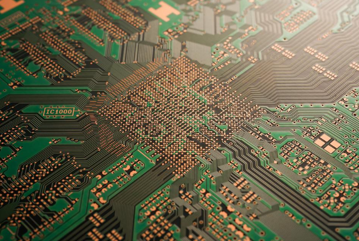
EM-888 is a high-speed printed circuit board with gold fingers. It is used in electronic devices that require high data transfer rates, such as telecommunications equipment, computer servers, and storage systems. It can support speeds of up to 8 Gbps. It is made of a multilayer stackup of Rogers material and features gold-plated copper traces. EM-888 is designed for use in high-speed applications such as data storage, servers, and networking equipment. It is also compatible with a variety of connectors and cables.
Material Consideration
The EM-888 high-speed PCB with gold finger mainly consists of a substrate, conductive pattern, and solder mask. The substrate is made of dielectric materials such as glass fiber or paper. Conductive patterns are made of copper foil laminated on the substrate. A solder mask is a layer of green or another color that covers the entire surface of the PCB except for the exposed areas of the conductive patterns.
The material used for EM-888 high-speed PCB with the gold finger is a special laminate for high-speed applications. The material consists of multiple layers of dielectric material and conductive materials. The dielectric material is used to insulate the conductive materials from each other and to provide a barrier between the electrical components on the board and the ground. The conductive materials connect the different electrical components on the board.
Dielectric Materials
The dielectric material in EM-888 high-speed PCB with the gold finger is typically a polyimide or FR-4. Polyamide is a strong, flexible, and heat-resistant material that can withstand the high temperatures generated by high-speed electronics. On the other hand, FR-4 is a fire-resistant material used in applications with a fire risk.
Conductive Materials
Copper or aluminum are the common conductive material used with gold. Copper is a good conductor of electricity and has a low resistance. Aluminum is also an excellent electrical conductor but has a higher resistance. The choice of conductive material depends on the application and the required electrical properties.
PCB Manufacturing Process
EM-888 is manufactured by a process called microelectronics lithography. This process uses light to create circuit patterns on a silicon wafer. The circuit patterns are then transferred to the EM-888 board using a photolithographic process.
Microelectronics Lithography
Microelectronics lithography is the process of creating patterns on semiconductor wafers or other materials that you will use to fabricate integrated circuits and other microelectronics devices. The patterns are created by selectively exposing the material's surface to an energy source, such as ultraviolet (UV) light, which causes certain areas to become more chemically reactive than others. The exposed areas can then be etched away, leaving behind the desired patterns.
Microelectronics lithography is a critical step in the manufacturing of semiconductor devices, and the quality of the patterns that are created can have a significant impact on the performance of the finished devices. For this reason, you must take great care to ensure that the lithography process is performed correctly.
One of the challenges in microelectronics lithography is that the patterns that need to be created are getting smaller and smaller as device manufacturers strive to pack more and more features into their products. This has necessitated the development of ever-more sophisticated lithography equipment and techniques. Another challenge is the need to create patterns with ever-greater levels of precision. This is necessary to ensure that the finished devices function correctly and perform as intended.
The microelectronics lithography process can be divided into several steps, which are described in more detail below:
- Wafer Preparation: The first step in the process is to prepare the wafer surface for lithography. This typically involves cleaning the surface and applying a special coating, known as a resist, which will be used to create the desired patterns.
- Pattern Creation: The next step is exposing the resist-coated wafer to an energy source, such as UV light, to create the desired patterns. This can be done using various lithography equipment, such as masks, stencils, or projection systems.
- Development: Once the patterns have been created, the resist must be developed to remove the exposed areas and leave behind the desired patterns.
- Etching: The next step is to etch away the exposed areas of the wafer using a chemical or plasma etching process. This will leave behind the desired patterns on the surface of the wafer.
- Cleaning: The final step is to clean the wafer surface and remove any residual resist or other contaminants.
Benefits of Using EM-888 High-Speed PCBs with Gold Fingers
EM-888 high-speed PCBs offer several benefits for use in high-speed applications. The Rogers material used in their construction provides excellent signal integrity, making them ideal for data-intensive applications. EM-888's gold fingers also provide superior electrical connectivity and durability compared to other types of printed circuit boards. The gold fingers are also resistant to corrosion and wear, making them ideal for high-speed data transfer applications.
The gold-plated copper traces also offer low resistance and high conductivity, which helps minimize signal loss. EM-888 also features various plating options, making them compatible with a wide range of connectors and cables.
Challenges associated with EM-888 High-Speed PCBs
Due to their high speed and data capacity, EM-888 high-speed PCBs can be difficult to work with. The boards are also susceptible to damage from ESD (electrostatic discharge). So, taking precautions when handling or working with these PCBs is essential. Gold fingers can also be delicate and require careful handling to avoid damage.
Despite these challenges, EM-888 high-speed PCBs with gold fingers offer several benefits that make them well suited for use in high-speed applications. Their excellent signal integrity and compatibility with various connectors and cables make them an ideal choice for many projects.
Wrapping Up
EM-888 High-Speed PCB With Gold Finger is perfect for your next project! It offers high speed and performance while also being able to handle a large number of signals. This makes it the ideal choice for any application that needs reliable signal transmission.


