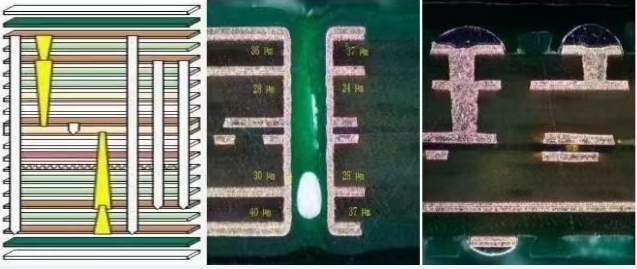
Are Buried Vias Filled?
Do buried vias need to be filled? What happens if they're not? This post will look at the benefits of filling buried vias, the consequences of not filling them, and some methods. By the end, you'll know whether or not your next design should include filled buried vias.
What Are Buried Vias?
Buried vias are a type of through-hole interconnect used in printed circuit boards (PCBs) that allow for electrical connection between layers of the board that are not on the same surface. Buried vias are not exposed on either the top or bottom layer of the PCB and are typically used to connect the inner layers of a multilayer PCB.
Buried vias are typically used in high-density interconnect (HDI) PCBs, boards with higher electrical components and circuitry than standard PCBs. HDI PCBs are used in various applications where space is limited, such as in cell phones and other handheld electronic devices.
The main advantages of using buried vias are that they do not require through-hole plating, which can be expensive and time-consuming, and they allow for a higher density of interconnections on the PCB. Buried vias are also less likely to cause signal crosstalk than other interconnect types.
Disadvantages of buried vias include that they are more challenging to fabricate than other types of interconnects and are incompatible with all PCB manufacturing processes. In addition, buried vias can be more expensive than different types of interconnects.
Are Buried Vias Filled?
The short answer to whether or not buried vias are filled is yes; they are typically filled with conductive material. This helps to create a low-impedance connection between the different layers of the PCB.
There are a few different methods that you can use to fill buried vias:
Conductive Epoxy
When vias connect different circuit board layers, it is essential to ensure that the vias are adequately filled with conductive material. This is typically accomplished by using a conductive epoxy. Conductive epoxy is available from many manufacturers, and the application will determine the specific product used. In general, the conductive epoxy should have a low viscosity to allow it to flow into the via, and it should be able to cure at room temperature.
Conductive epoxy is typically dispensed via a syringe or dispensing needle. The amount of epoxy dispensed will be determined by the size of the via. It is essential to ensure that the epoxy fills the via and that there are no voids. Once the epoxy has been dispensed, it will typically take several hours to cure.
Once the epoxy has cured, it will need to be trimmed flush with the surface of the circuit board. This can be accomplished using a sharp knife or a pair of scissors. It is essential to be careful not to damage the circuitry on the board's surface. After the epoxy has been trimmed, the vias can be used to connect different layers of the circuit board. This will allow signals to pass between the other layers.
Electrodeposition
Electrodeposition can be used to fill buried vias with conductive powder or paste. This process involves passing an electric current through the powder or paste, which causes it to be deposited onto the surfaces of the vias. The advantages of this method include its high accuracy and ability to fill large numbers of vias in a short period.
Electrodeposition is widely used for filling buried vias with conductive powder or paste. It has many advantages, including its high accuracy and ability to fill large numbers of vias in a short period. This method involves passing an electric current through the powder or paste, which causes it to be deposited onto the surfaces of the vias.
This technique is often used with other methods, such as chemical or physical vapor deposition, to create a conductive filling that fills the via. This ensures that no voids or air pockets are present, leading to electrical problems. Depending on the application, you can control the electrodeposition process to deposit different material thicknesses. For example, you may require thicker coatings for vias that will experience high levels of electrical current.
Electroplating
There are two ways to fill buried vias by electroplating, and each has its benefits and drawbacks. The first method, known as the batch process, involves filling a tank with an electrolyte solution and then submerging the PCBs in the tank. This method is typically used for small-scale production runs, as it is not very efficient for large-scale production. The second method, the inline process, involves plating the buried vias as the PCBs are being fabricated. This method is more efficient than the batch process but can be more expensive.
The benefits of filling buried vias by electroplating include increased circuit density and improved electrical performance. The advanced circuit density is because more vias can be placed in a given area when they are filled by electroplating. This allows for smaller and more compact PCBs. The improved electrical performance is because electroplated vias have lower resistance than non-electroplated vias. This means that they can carry more current and provide better signal integrity.
The drawbacks of filling buried vias by electroplating include the increased cost and the need for special equipment. The increased cost is because more chemicals are required for the process. Special equipment is needed because the inline process requires a plating line, which can be expensive.
The method used to fill the buried will depend on the application and the requirements of the PCB. For example, suppose the PCB needs to be able to withstand high temperatures. In that case, a different filling material may be used than if the PCB is for a lower-temperature application.
Wrapping Up
Buried vias are typically filled with conductive material to create a low-impedance connection between the different layers of the PCB. The most common method for filling buried vias is to use a conductive epoxy, but other methods include using conductive powder or paste or electroplating the via. The technique used to fill the buried will depend on the application and the requirements of the PCB.


