Flex circuits: Innovations and Processes
The use of flex circuits as solutions for various applications has changed the course of history. Their high-density capabilities allow us to implement various physical changes using small electronic components. In other words, they allow us to interface with the digital world.
Thanks to recent advancements and innovations in technology, flex circuits have become more robust with constant growth over the years.
A Primer on Flex Circuits
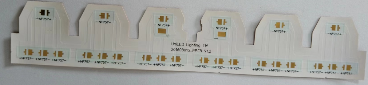
Flex PCBs are made from thin insulating polymer films with a pattern of conductive traces mounted onto a substance. There are several types of flex circuits, including single-sided flex, double sided flex, multi-layer flex, and rigid flex circuits.
The basic materials used in flexible circuits are as follows:
Conductor: To allow the flow of electricity. The most common conductor is copper but aluminum and carbon may be utilized in some cases.
Adhesives: Adhesives are used for surface mount component bonding. It is important for adhesives to be based on the use of customers' needs and the thickness of conductors. Popular adhesives include acrylic, PSAs, and epoxy.
Insulators: Insulators are used to separate circuit components from each other by forming a barrier between energized parts of the circuit and restricting the flow of electricity to conducting paths.
Flex circuits have enabled designers to embark on highly creative projects that utilize 3D configurations. Although their flexibility has allowed for use in various applications, flex circuits come with unique design challenges that can disrupt a device’s viability.
Designs have tackled these challenges by utilizing flex-supporting technologies that facilitate large-scale production of flex PCBs without sacrificing quality and output. Flex PCB manufacturers are pivoting to advanced techniques to ensure quality, yield, and market competitiveness of their circuits.
Flexible Printed Circuits
Flexible printed circuits require a unique manufacturing process that has been meticulously developed over the past ten years to support the production of flexible PCBs. A major improvement is related to how manufacturers handle traditional sheet of sheet materials. Moreover, the use of automated roll to roll processes are further refining the flex PCB production process to meet the growing demands of the market.
Let’s take a look at various technologies used with flex circuits.
CAM and CAD Solutions for Flex PCBs
Manufacturers use advanced design for manufacturing (DFM) tools for flex circuits to troubleshoot and eliminate problems encountered in the design stage.
These special tools have fully automated otherwise redundant and manual processes that were prone to errors and took too long to produce. DFM tools facilitate various processes such as automated coverlay, solder mask optimization, and surface smoothing, ensuring higher quality, accuracy, and longevity.
Designers can gain even more control over flex circuits with the help of based flex circuit designs. These tools are used to review the design at various stages of the manufacturing process.
They can be used to check problems related to stiffeners, bend areas, air gaps, conductive masks, trace overlaps, and frequent moving parts.
All kinds of CAD and CAM design tools such as EasyEDA and KiCAD EDA are used to aid electronic engineers in designing layouts for circuits.
Laser Drilling Systems
A major improvement in flex PCB design technology is using laser-based systems. Simply put, a laser source is used to provide drilling instead of outdated and error-prone mechanical drill bits used in conventional manufacturing systems.
Laser drilling systems can be configured to specific wavelengths based on the material being cut. They use a high-energy application that vaporizes the material. This process may leave a slight charring on the edge of the circuit because of the resulting heat.
Laser sources can also be used to a specific diameter. Most systems have a working platen used to secure the tool into position. A laser head is then controlled in the X and Z axes, allowing it to move at a very high degree of accuracy throughout the circuit.
A key advantage of laser systems is that they can drill holes of very small diameters. Mechanical drill bits are limited to sizes of 0.006”. Any smaller, and the drill bits can be worn out very quickly. Besides, they can be very expensive for businesses with smaller budgets.
In recent years, laser drilling supports have been modified for use with for roll to roll production mode. This will be discussed below.
Roll to Roll Processing
Although roll-to-roll processing is not cheap, they streamline the fabrication method for flex PCBs. Most electronics are fabricated with R2R technology, including mobile phones, computers, and various home appliances.
The biggest advantage of using R2R infrastructure is that it eliminates flex damage, increasing yields and quality.
The Use of Laser Direct Imaging (LDI)
Another major advancement is the use of laser direct imaging to use with sheet-based imaging for rigid flex materials. LDI systems overcome a number of problems thanks to the use of:
Depth of Field (DoF) optics
DoF optics are used to create fine lines on flex materials where the surface may not be flat. Support for surface height variations of 100 to 300 is provided. Combining LDI with Large Scale Optics (LSO) allows a DoF of over 300 micrometers, ensuring greater uniformity on the flex surface.
Alternatives to DoF systems are less accurate and do not support surface variations of over 100 micrometers, resulting in inferior line quality and lack of uniformity.
Distortion Compensation
Distortion compensation systems can minimize the deformation of flex sheets during production. This is done by individually measuring each flex sheet and imaging it with a corrected image. This ensures accurate alignment of circuit patterns with drilled vias. Drilling compensation is only possible with the help of a digital direct imagine solution. Manual processes are simply not accurate enough to accurately correct the pattern image.
These systems are incredibly accurate and support high quality flex PCB production.
Automated Optical Inspection (AOI)
Most flex PCBs are either single sided or double sided. These circuits did not undergo Automated Optical Inspection. However, the industry is embracing the use of AOI in recent years for higher quality control of single and double sided flex PCBs. AOIs are especially useful with smartphone interconnects.
Advanced AOI tools are empowering manufacturers with accurate imaging capabilities, allowing flex PCBs to be thoroughly scanned and minimize errors.
Wrapping Up
Flex PCBs are incredibly useful in electronics, including smartphones and computers. They leverage advanced laser drilling, CAM and CAD tools, and R2R infrastructure to empower designers with highly versatile flex circuits.
Need help with your next project? Get in touch with flex PCB experts at Hemeixin PCB here.


