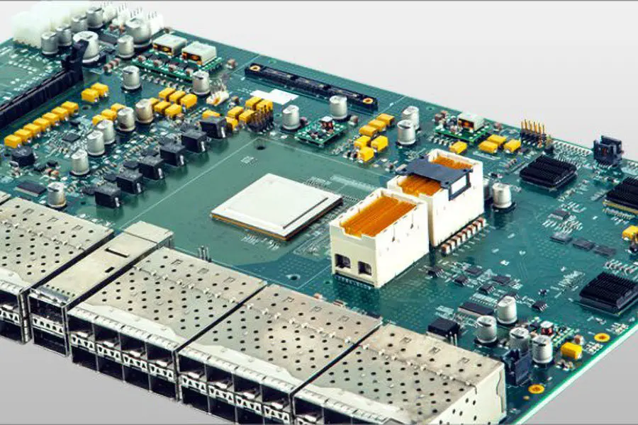
HDI PCB Routing Challenges and Tips
Routing PCBs is an integral part of any PCB design. The layout and design should be done carefully and patiently to get the optimum result. Routing a PCB is a difficult task, not only because routing tools are complex but also because PCB routing is an art – requiring experience, knowledge, skills, and brains. These challenges can be tedious to solve and time-consuming.
If you are building a PCB, knowing a few essential tips can help you avoid these setbacks. This post provides expert tips on how to choose the right tools, how to work efficiently and effectively, and how to avoid common pitfalls during PCB routing.
What Is HDI Routing?
HDI routing is an interconnect technology that allows you to route your board using the horizontal and vertical layers of the board. With HDI routing, a single trace can cross over other traces in both directions and penetrate through a plane. This means that all planes are connected.
This type of routing is ideal for designs where signal integrity and quality are critical. However, some people find it challenging to use, and it is not always needed or recommended for every design.
The main advantage of HDI PCB routing is its ability to take advantage of the increased current carrying capacity provided by wider traces. For example, if you have two layers in your PCB that are separated by a third layer, you can use this method to route all three layers at once rather than having to route each layer separately. This allows traces on one layer to connect directly with traces on another without needing any vias or jumpers between them.
HDI Routing: Primary Types
There are two types of HDI routing: Simple and Advanced.
Simple HDI Routing
Simple HDI routing works by creating an idealized version of your board which is then "mapped" onto your physical board. The actual routing step is the same as regular single-sided routing. It is just that the initial placement can be quite different than what you see in the schematic editor.
Advanced HDI Routing
Advanced HDI routing uses a different approach, where it tries to fill in any gaps between tracks even before they are routed. This means that when it comes time to route, all the pads will be connected by traces, even if there are obstacles in between them on your physical board. This allows for much more flexibility when placing your components on your board since it does not matter if there are holes between the pads.
Typical HDI Routing Setbacks and Prevention Tips
Signal Integrity
Signal integrity measures how well signals travel from one point to another on a PCB. Signal integrity is critical because it affects the performance of your product and its ability to function correctly. If there are problems with your PCB's signal integrity, you could have issues such as high-frequency noise or electromagnetic interference (EMI). These can cause problems such as reduced bandwidth, data loss, and even physical damage to sensitive components in your product.
Always ensure that the PCB layout must be designed so that the signals do not encounter impedance mismatches or reflections that could cause unwanted reflections on the signal path.
Trace Width
Trace width is one of the most critical factors in HDI PCB routing. When using a narrow trace width, it will be easier to route the nets. Also, with the help of narrow trace width, you can reduce the number of vias required in your design. But on the other hand, if you use a wide trace width, it will be difficult for you to route your network and increase the number of vias required in your design. It is essential to minimize trace widths since they will be stacked together with other layers. This can be achieved by reducing the diameter and increasing spacing as much as possible.
Ground Planes
The ground plane is a set of copper traces on the PCB that provide a low resistance path to the ground. The ground plane also helps to block noise and interference. If there is not enough copper in a design, either because it was not planned or because the manufacturer did not include enough, then this can cause problems with signal integrity. The best way to overcome this is by creating a copper plane that overlays the entire board. This will ensure sufficient power distribution and reduce noise on your circuit.
Number of Vias
The number of vias required in the design is another critical factor in HDI PCB routing. If you have many vias in your design, it will be difficult for you to route your nets and increase the cost of manufacturing. To avoid this situation, you should minimize the number of vias in your design by using as many alternative routes as possible for signal routing.
Inductive Coupling
Inductive coupling is a phenomenon that occurs when a signal passes through a loop of wire. The magnetic field created by the current induces a voltage in nearby loops of wire. This means that any trace on your PCB that is close to another trace can act as an antenna and pick up interference.
The solution is to keep traces as far apart as possible but not so far that they do not fit on the board. Also, keep your signal traces close together (within 10 mils or 0.025mm), which will help prevent inductive coupling from occurring between them.
Power Planes
Power planes distribute power from the power supply through the board. Some designs have multiple planes to keep each section of the board at the same voltage level and reduce noise on each section of the board. If a design uses just one layer for power distribution, there will not be enough current capacity to handle high-speed signals or high current loads such as switching regulators and other power supplies. In this case, use multiple layers for power distribution so as not to overload any one layer of copper traces and cause them to break down or overheat due to excess current flow.
Key Takeaway
Every designer knows that routing is a never-ending learning process. There is always something new to try, some new technique to master. This guide is designed to give you some helpful insight and tips while still learning the basics of HDI PCB routing techniques.
Hopefully, these tips provide a valuable starting point for using HDI boards to create challenging yet highly functional printed circuit boards. If you want to learn about HDI PCB design guidelines, Hemeixin HDI PCB is an excellent place to start.


