Managing High-Density Vias in HDI PCB Design
High-Density Interconnect (HDI) PCBs are becoming more and more popular as layout engineers seek to make the most of the limited board in the electronics industry. The popularity of HDI technology is increasing due to its low-cost developmental process, ability to increase signal density, and design flexibility.
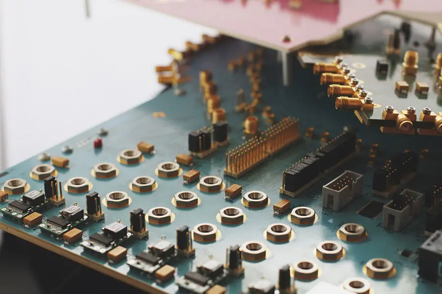
If you are a designer working with high-density interconnect (HDI) boards, you are probably well aware of the challenges of designing for high-density vias (HDV). Vias connect the top and bottom layers of a multilayer PCB. The primary purpose of the via is to transfer the required signal from one layer to another. However, if not correctly designed and implemented, there are instances when vias can affect different electrical parameters.
A board design has much to consider just getting the significant features to work together harmoniously. Added complexity comes into play when factors such as performance and reliability are also considered. This guide will explore the various aspects and tips to overcome challenges associated with high-density vias in HDI PCB design.
The Need for High-Density Vias in HDI PCB Design
In the past, the use of high-density vias (HDV) in printed circuit boards (PCBs) was limited due to the issues they caused during manufacturing and assembly. However, with technological improvements, these issues have been resolved, and HDV can now be used in many applications that were previously impractical.
The most significant advantage of using HDV is their ability to reduce the number of components by allowing them to be placed closer together. This reduces both their cost and size. In addition, they can also improve signal integrity by reducing crosstalk between adjacent traces.
HDI PCB Design: Managing High-Density Vias
Add Vias Only Where Needed
The number of via holes in an HDI PCB design is the primary factor that determines whether your assembly will pass or fail. You might think that adding more vias will decrease impedance mismatches between layers, but this is not necessarily true.
For example, if you put too many vias into a network of traces that run perpendicular to each other on different layers, it could create more impedance mismatches than if you had added fewer vias between those same traces.
Select the Best Fit via Size
The most common mistake designers make when creating an HDI board is using too many large vias. This results in a higher impedance mismatch and can cause problems with signal integrity issues such as crosstalk and signal degradation. To avoid this issue, selecting the right-sized via for each location within your design is important.
For example, larger surface-mount vias should be used where there are multiple layers that need to interconnect with each other, as shown above. This will ensure that each layer has an adequate amount of copper, which helps reduce impedance mismatches and ensures high signal integrity throughout your board.
Keep High-Density Vias Isolated from Each Other and Other Components
In addition to using the correct sized vias, keeping them isolated from each other and other components on the board is essential so that they do not fall out against one another or affect sensitive portions of your design. While this may seem obvious, many designs can suffer from this issue if not designed properly.
There are two main ways to ensure that your high-density vias do not short out. The first is to use isolation routing techniques such as via-in-pad (VIP). These techniques are used in conjunction with pads on top of each pad on your board, where you place your high density. This way, any electrical current will go through this pad first before reaching underneath it. The second method uses a non-conductive material such as FR4 between two high-density vias, which ultimately prevents their electrical current from reaching one another.
Use a Smaller Drill Size
Another way to optimize your design for high-density vias is by using a smaller drill size when drilling holes. This will reduce impedance mismatches between signals and vias which will help improve signal quality overall. You should also use a smaller diameter drill bit if possible because it will give you more flexibility when placing holes on your board layout and allow you to place them closer together than if you were using a larger diameter drill bit.
Enlarge via Pads
Another way to help improve signal integrity on an HDI board is by enlarging the via pads around each via location. This will allow you more space around the via itself, allowing you to use larger diameter copper traces instead of small ones, which can help reduce impedance mismatches between layers and improve the overall performance of your circuit board.
However, you should remember that this may affect your board's thermal performance, so it is essential to ensure that you have enough thermal relief between pads and traces to prevent overheating damage.
Shorten Trace Lengths to the Via
Since high-density vias can be difficult to route, it is recommended that you shorten trace lengths to them as much as possible. This will help reduce the amount of copper consumed by the via itself and free up more room for routing other traces around it. It should also be noted that smaller vias tend to have lower inductance values which improve signal quality because it reduces crosstalk between traces sharing the same via interconnects.
Use a Multilayer Board Design
To optimize your design for high-density vias, it is recommended that you use a multilayer board design whenever possible. This will allow you to place signals on different layers, so they do not compete with each other for space on a single layer. For example, if you want to connect two signals on opposite sides of the board, placing them on different layers will give them more space which will help reduce impedance mismatches between them and improve signal quality overall.
The Bottom Line
Managing high-density vias is not so much a technical issue. It all comes down to proper planning. Avoiding errors like mistakenly placed, misplaced, and missing vias is easy. It requires a systematic approach to resolve these problems early on in the design process, rather than trying to fix them after you have sent the design off for fabrication.
We hope this guide will clarify any confusion and provide helpful tips for dealing with these challenging boards. However, it is worth your time to learn as much as you can about them from Hemeixin and make good use of them in your projects—as long as you understand the caveats.


