Layout Tips for Flex PCB Design
Flex PCBs are very much in use in many different markets, so it is obvious that they provide us with some extra benefits compared to the conventional rigid PCB. The benefits include thinner designs, better shock resistance, and the flexibility to move your boards out of the way without damaging them. A common problem with flex PCBs is that they can get out of place during assembly or installation. This causes poor connections as well as a less-than-professional look.
There are many things you have to know before starting a layout design if you want it to run correctly when you are done. This guide looks at some simple ways to layout flex PCBs to help fix these problems.
Flex PCB Layout Tips
A Flex PCB's layout is as important as the design itself. The following tips will help you create a better-designed Flex PCB.
Keep It Simple
The simpler the design, the easier it will be to produce and assemble. Don't complicate things with unnecessary elements or features. This can make the manufacturing process more difficult and increase costs.
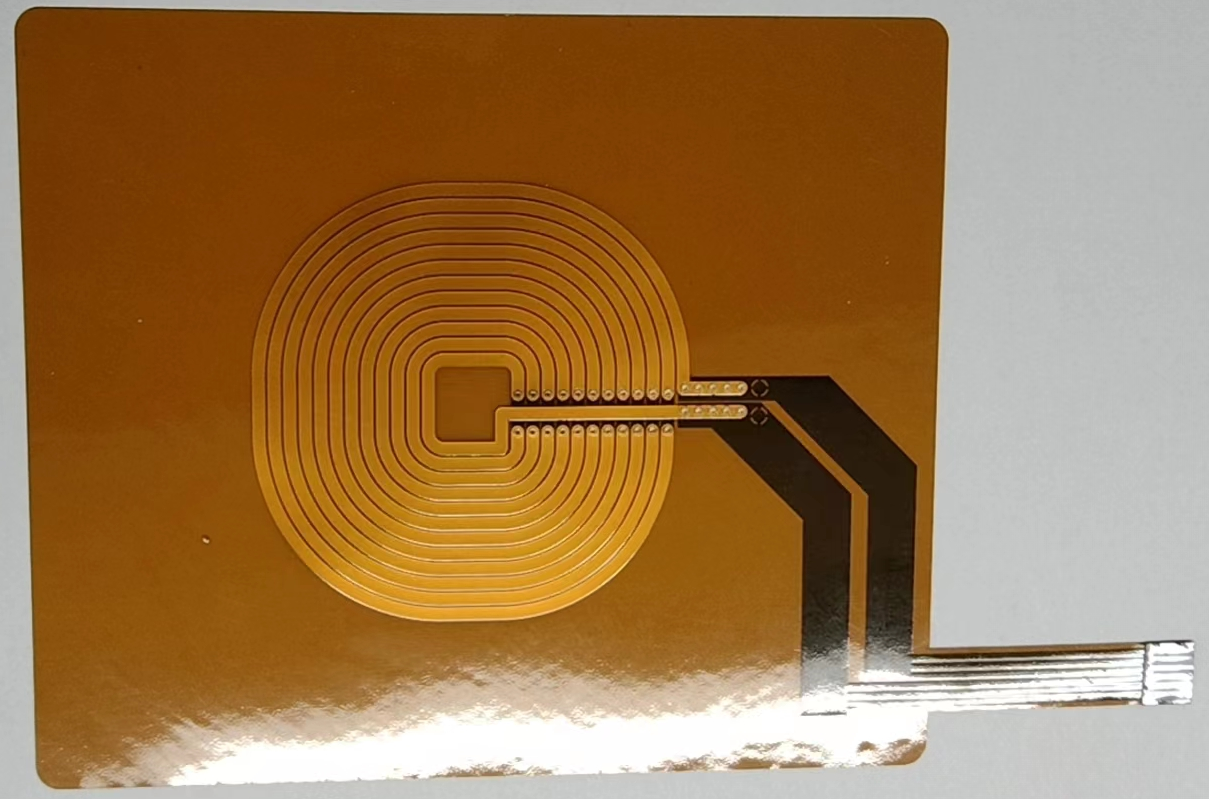
Use Sharp Corners
Corners that are too rounded can cause problems during assembly, especially when using ultrasonic welding machines. Sharp corners give you a better seal around the joint, which is essential for waterproofing and other functions in an electronic device.
Minimize Trace Lengths
When designing a Flex PCB, keep trace lengths as short as possible while maintaining adequate current carrying capacity. This will reduce the overall cost by reducing the need for thicker copper traces or expensive through-hole components like relays or power transistors.
Avoid Using Vias
Vias connect two circuit board layers by passing through them from one layer to another. But they are not suitable for flex circuits because they make the circuit board more rigid, which is not desirable for flexible boards. If you need to connect two layers of your flex circuit board, choose other options such as jumper wires or microvias instead of vias.
Keep Track of Layers
Flexible circuit boards can have several layers depending on the application requirements. For example, it can be a 2 or 3-layer flex circuit board, but in some cases, it can be more than 5 layers. So it is vital to keep track of all the layers while laying out your design. The reason behind this is that you do not want any overlap between the layers, as this will affect the flexibility of your product. Also, ensure that there is enough space between each layer so that you do not have any issues with soldering and assembly later on during the manufacturing process.
Keep Ground Planes Close Together
When designing a flex PCB, keeping all the ground planes close together is essential. This will help reduce crosstalk between traces on different layers and prevent interference from other circuits around your design.
Use Thick Copper
The use of thick copper in flex PCB design is an essential factor in the success of your product. The thickness of the copper layer directly impacts the performance and reliability of your flex PCB.
A thin copper layer will cause many problems for you during prototyping and manufacturing. For example, the thinner copper traces will have higher resistance and lower current carrying capacity. This may lead to overheating or short-circuit problems during the operation of your device. In addition, if you design too thin copper layers, they will be easily damaged by mechanical stress or surface abrasion while the handling and testing stages.
The most common copper thickness in flex PCB design is 1 ounce (oz). However, by using thicker copper layers such as 2 oz or 3 oz instead of 1 oz when designing flex PCBs, you can increase the reliability and performance of the PCB.
Route Traces at Different Levels
Using different traces at different levels will make the routing process easy and fast. This can be achieved by using wider traces in the outer layers and narrower traces in the inner layers. This will help reduce the number of vias required in your design and your total cost.
Consider Adding Stiffeners to Long and Narrow Boards
The use of stiffeners in Flex PCB is a common practice. It is used to reinforce the long and narrow boards, typically bent during the assembly process. The following are some reasons why you should consider adding stiffeners to your long and narrow boards:
- Stiffeners will prevent warping during the assembly process. Warping can cause poor contact between components and traces, leading to reliability problems.
- Stiffeners will make it easier to handle the board during assembly, testing, and final packaging.
- Stiffeners will make it easier for automated pick-and-place operations to handle the board during assembly.
Stiffeners can be either single-sided or double-sided, depending on your design requirements. Double-sided stiffeners can provide mechanical stability on both sides of the board and may be more robust than single-sided designs because of their symmetrical nature and more material used in manufacture.
The size, thickness, and height of the stiffener will vary based on several factors:
PCB Thickness and Density - Thinner PCBs require smaller stiffeners, while thicker ones require larger ones.
Cable Routing - The more extensive the cable channel through the PCB stackup, the larger the stiffener should be.
Panel Size - Larger panels require bigger stiffeners, so they do not bow out when mounted.
PCB Standoff Location - The farther away from the panel edge a standoff is located, the larger it needs to be.
Key Takeaway
While flex PCB design is often the best option for a project, it carries a few challenges that you might not encounter in other circuit designs. To get a successful print, it is best to know what those challenges are upfront. You can then work to avoid them during the design and revision process—and if they do crop up, you can be better prepared to handle them before it is too late. With this handy list of things to look out for, we hope your flex PCB design project goes smoothly from concept to completion. For a more thorough understanding of the subject, read Hemeixin's design guidelines for flexible circuits.


