Multilayer PCB Design: HDI Stackup Demystified
When designing a PCB, the multilayer PCB stack-up is one of the most important decisions. It ultimately decides the route your electrical signals will take through the PCB and how fast those signals can travel. When choosing a stack-up, many key considerations include how complex your desired termination pattern is. There are trade-offs in each choice. After this discussion, you should have a basic understanding of the stacks-ups used in HDI PCB design.
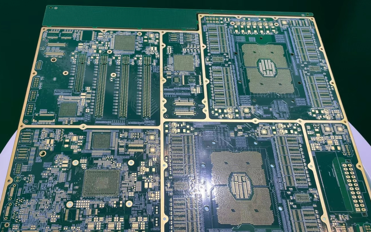
HDI PCB Stackup
HDI PCB stackup is a method of stacking HDI boards from top to bottom on each other and using the prepreg material to hold them together. This is commonly done using glass fiber or carbon fiber reinforced plastics (GRP) in a stackup.
The holes are drilled through the top layer and into the bottom layer of the stackup at a predetermined pattern and spacing. Then the hole is reamed out larger than the diameter of the fastener (usually 3/16" or 1/4") so that it can be tapped into place with an anti-seize compound applied to it. The fastener will then hold all layers together while curing takes place.
This stacking method allows for much more complex shapes to be built up than would be possible with a manual layup. However, it requires additional equipment such as a drill press (or at least a drill), reamers, taps, and dies for threading fasteners into place.
Multilayer HDI PCB Stackup
There are many different types of HDI PCB stackups. Some are more common than others, but all have their place in the design process.
The most prevalent type of HDI PCB stackup is called multilayer stackup. This means that there will be multiple layers of copper within the board. They may be stacked vertically or horizontally, depending on the specific requirements of your design. The most common form is where the bottom layer comprises ground planes and other components that need to be connected for power distribution purposes. The next layer up would be your power plane, followed by signal traces on top of that. These three layers are then connected using vias, holes drilled through the board so that you can connect different layers without using jumpers or other methods, which can cause issues with signal integrity.
Multilayer HDI PCBs stackup can be made using either through-hole technology or surface mount technology (SMT). The choice between these two methods depends on how much space is available on the board and what components need to be mounted. Through-hole mounting requires more space than SMT mounting, so if you use larger components or want to install many devices onto your board, then SMT may be better suited for your needs.
The main structure of HDI PCB stackup includes:
- A conductive metal layer (aluminum or copper alloy) is used as the ground plane.
- Signal layer (copper foil), which is used for signal transmission.
- A dielectric layer (preg), which separates the two layers above and prevents them from touching each other
- Grounding layer (silkscreen), which ensures that all parts of the circuit boards are connected to the ground plane through conductive metal
- Insulation layer (glass fiber cloth), which insulates between layers
- Solder mask cover layer (satin solder mask), which protects components from corrosion during soldering
Multilayer HDI PCB Stackups Uses
Multilayer HDI PCB stackups are designed with a specific purpose in mind. They are designed to support the application requirements of different electronics systems. They can be used for anything from high-frequency RF circuits to low voltage power supplies and everything in between. Here are some examples:
Large Ground Planes
A large ground plane is an important feature of any high-performance circuit board. It allows for better heat dissipation and provides more surface area to pass signals. However, as you add more and more layers to your ground plane, it becomes exponentially harder to drill holes through it. With a multilayer HDI stackup, you can have a large ground plane without worrying about drilling holes through it.
High-Frequency Circuits
High-frequency circuits require short trace lengths between components to minimize signal degradation caused by capacitance. A multilayer HDI stackup makes it possible to route wires very closely without increasing parasitic inductance or capacitance. This can help improve the performance of your circuit board at high frequencies.
High Density Interconnects
High density interconnects provide more routing options while eliminating vias-which are used when multiple components need to be connected on a single layer of copper foil. This reduces cost and improves reliability by removing vulnerable connections from the board itself and placing them inside the connector, where they cannot fail.
Multilayer HDI PCB Stackups Important Considerations
Multilayer HDI PCB stackups are very complex and require a lot of preparation. The designer has to take into account different things when designing them, such as:
Layer Count
The number of layers on an HDI board depends on the application, but it is usually between 2 and 6 layers.
The number of layers in an HDI board depends on its size and complexity; therefore, it is recommended to start with a small design before moving to bigger ones.
Layers Organization
The layers organization on an HDI board is critical for its performance because you must consider all possible failure scenarios during production or operation.
For example, if you have three layers, two core, and one ground, and you do not have any vertical interconnections between them, if one layer fails, then all other layers will be affected by this failure as well because they are not connected vertically through vias (no current flow).
Layer Thickness
The thickness of each layer can vary depending on the application. For example, if you need a thicker ground plane on your board, you can add more copper than usual (typically 0.6mm). If you want thinner traces, use less copper (0.2mm).
Final Word
We hope this guide is useful if you find yourself designing complicated HDI PCBs. The multilayer aspect can make or break the final product, and knowing the effect each layer will have in advance is an easy way to keep your design simple. If you are interested in learning more about HDI PCB design guidelines, you should check out Hemeixin's HDI PCB blog post.


