What Are High Density Interconnect PCBs?
As computer technology rapidly evolved over the past decades, making faster and more efficient circuit boards became necessary. The discovery of high-density interconnects PCBs has created a new standard for circuit boards.
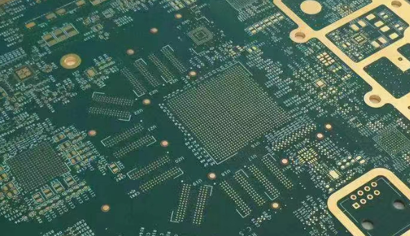
High density interconnects (HDI) PCBs are a growing trend in modern board design and have revolutionized the manufacturing of electric devices. It is a massive leap forward from the most common PCBs, called conventional or single-layer PCBs. With the growth of specialized microprocessors and high-end IPAs, companies are trying to get more done with less. HDI PCBs allow data and signals to be transferred in smaller, more compact spaces.
If you are developing a new electronic product and are looking for a cheaper low-cost solution than the conventional PCB, HDI boards could be precisely what you need. To help you better understand, this guide will explain what High density interconnect PCBs are and how they are used.
High Density Interconnect PCBs: Brief Overview
High-density interconnects PCBs differ from traditional single-layer PCBs because they have more than one layer. The number of layers can vary from two to five, although three and four-layer boards are the most common. Each layer is printed with a set of conductive tracks, which allow current to flow between components on different layers.
The main reason for using high-density interconnect PCBs is that they allow more components to fit on a single board. This makes it possible to create smaller, more efficient devices while maintaining the same level of performance as larger devices. Besides, they have wide-ranging applications in various industries but have primarily become popular in the data storage market owing to the need for storing information in ever-shrinking dimensions.
Advantages of HDI PCBs
Here are the advantages of HDI over traditional PCBs:
Reduced Space Requirements – HDI PCB boards require less space than conventional PCBs when used in conjunction with other technologies such as 3D stacking or interposers. This makes them ideal for use in applications where space is at a premium, such as smartphones and tablet computers.
Higher Throughput – HDI boards can be processed faster than traditional boards because there is less handling and sorting required during manufacture and assembly, so there is less opportunity for damage or misalignment during processing.
Better Quality Control – With fewer steps in the manufacturing process, there is less opportunity for human error to occur during production and assembly.
Lower Failure Rate – The materials used in HDI boards have a longer life cycle than those used in traditional PCBs, so they are more durable overall.
HDI PCB Common Applications
HDI PCBs have a wide range of applications; however, there are some areas where they are used more than others. The following are the typical applications for HDI PCBs:
Automotive Electronics
These include sensors and actuators installed in automobiles. They control various functions such as steering, braking, and acceleration.
Industrial control panels and automation systems
HDI PCBs are often used to make industrial control panels and automation systems that require high levels of reliability. These include medical equipment, power plants, oil refineries and other industrial facilities where uptime is essential.
Telecommunications Equipment
High-density interconnection boards (HDI) are extensively used in telecommunications equipment like routers, switches and servers, where high performance is required at a low cost per square foot.
Medical Equipment
This includes medical imaging systems such as X-ray machines, MRI scanners, and medical diagnostic equipment such as blood analyzers.
HDI PCB Layers Stackup
The number of layers on an HDI board has become increasingly important due to the need for higher bandwidths and densities in electronic devices. Today's HDI boards range from two through six or more layers, with each layer having specific functions based on how engineers designed them. A typical high-density interconnect PCB stack up includes four main layers. From the outside, the PCB stackup looks like this:
Layer 1: Copper Layer
This is the most important layer because it is where signal traces and power/ground connections are routed. It is also where vias are placed to connect between layers.
Layer 2: Ground Plane
This single-sided copper layer provides a large surface for heat dissipation. It also helps keep signals from interfering by providing a barrier between them.
Layer 3: Signal Layer
This is where all signal traces go — typically one row per component pin and 8 or 10 pins per component. Each row has its ground plane on both sides.
Layer 4: Component Pads (Top and Bottom)
Each component pad has two sides: one connects to the corresponding via on Layer 1, and the other connects to the corresponding pad on Layer 3 through an opening in the solder mask.
Few Design Tips
The following are some crucial factors that should be considered while designing high-density interconnect PCBs:
Minimize Solder Mask Thickness
To increase the number of components on a board, you must reduce the solder mask thickness. This can be achieved by reducing the size of your artwork or by using a smaller solder mask font.
Use High-Density Vias
High-density vias (HDV) are a popular technique for improving signal integrity, especially in high-frequency signals, because they provide better impedance matching between layers. Depending upon your requirements, HDV can be used for both through holes or blind vias.
Design with Multiple Ground Planes
It is always recommended to have multiple ground planes on your board to easily route signals without having any electrical conflicts with each other. This also helps improve signal integrity and reduces crosstalk between signals by providing better impedance matching between layers.
Summary
In short, HDI PCB boards are more than just what the name implies; they represent a new paradigm of dense component layout and routing. From the primary function of supplying power to a circuit to housing the most intricate components and their connecting wires, HDI PCBs are a critical part of many modern circuit designs. Hopefully, by now, you have a basic understanding of HDI PCBs and why they are helpful in some circuit applications.
However, HDI boards are not without their pitfalls; specific fabrication processes must be followed to ensure their effectiveness. So long as manufacturers take these processes into account, you can expect to see an increase in HDI board design over the next few years. To get high-quality HDI PCBs manufactured, check out Hemeixin.


