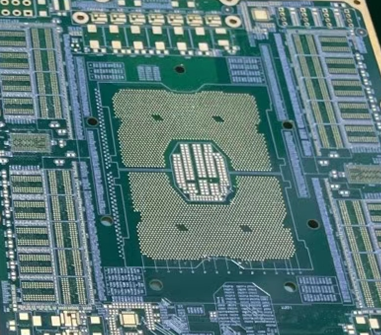
What is Conductive and Non-conductive Via fill in HDI PCB?
HDI PCB designers are often confused when it comes to via fills. They have a choice between conductive via filling and non conductive via filling. Via hole plugging is often used to make surface mounts more reliable.
Other advantages include higher quality yields of the assembly and better reliability of the micro via PCB by reducing the likelihood of trapped substances in the via.
Let’s quickly go over the two choices that confuse designers.
Conductive Via Fill
Conductive via fills are used to carry large amounts of current or heat to another layer of HDI PCB. They usually have copper particles dispersed around the epoxy to provide more electrical and thermal conductivity. Conductive via fills are used to provide more conductivity to applications.
There are a few choices for conductive via fill materials: Tatsuto AE3030 and DuPont CB100. Both use silver coated copper particles filled with epoxy matrix.
The main difference between both materials is the overall particulate size and CTE (coefficient of thermal expansion). The particulate size of CB100 material is larger with a higher CTE. Furthermore, CB100 has been around for longer and is more popular with designers.
Advantages of Conductive Via Fills
Here are some of the main benefits of using conductive via fills:
- Allows heat transfer when other methods are not practical.
- Increase the current carrying capacity of HDI PCB circuits because of higher thermal conductivity (has a conductivity of 5 to 14 W/mK, which is considerably higher than non-conductive via fills).
Disadvantages of Conductive Via Fills
- Copper plating and copper pad are relatively unstable inside the via hole barrel. This is because of the differences in CTE (coefficient of thermal expansion) of the conductive laminate and material surrounding the via fill. When the HDI PCB goes through multiple thermal cycles, the metal will expand due to exposure to the heat more rapidly than the laminate. This can lead to fractures developing between the via barrel and the pad.
- The thermal conductivity of conductive via fills is not very high. This means you may have to add more vias to increase the thermal conductivity of the PCB.
- Conductive via fills are more expensive to use than non conductive via filling
- Very few fabricators can use conductive via fils because of low demand in the market
Non-Conductive Via Fills
The term non-conductive suggests that the via fill is a poor conductor of electricity or that it doesn't allow any current to pass. This is not true. The via will like any other electronic component in the PCB.
Non-conductive via fills have a thermal conductivity of around 0.25 W/mK compared to 3.5 W/mK of conductive via fills. For perspective, the thermal conductivity of electroplated copper is more than 250 W/mK.
Non-conductive via fills are usually used for via in pad designs to prevent the excess solder from wicking down into the via hole during reflow applications.
The two most popular products for non-conductive via fills are San-Ei Kagaku PHP-900 epoxy and Peters PP2795 epoxy. The former has been available for a longer period of time. However, San-Ei has taken the market lead because it provides a superior CTE match between HDI PCB laminates.
Advantages of Using Non-Conductive Via Plugging
- They prevent the solder and other substances from wicking away and entering the via.
- Provide structural support to pads.
- Improve the longevity and stability of via and pad because the CTE value of the filling material and laminate are similar compared to conductive via fills.
Which One Should You Choose: Conductive or Non Conductive Via Fill?
Before we dig in, let’s be upfront about the comparison - it depends on the application. There is no cut and dry answer when it comes to choosing between conductive and non conductive via fills.
Here are a few things you should consider when choosing between the two via fill options.
Budget - You want more bang for your buck while maximizing the performance of your HDI PCB. You don’t want to overpay for a solution that is redundant.
Application - You want a solution that aligns best with your application and its usage scenarios.
Design Simplification - Your goal should be to simplify the design as much as possible.
A major consideration is to keep the CTE value as close as possible with the surrounding laminate material. This is extremely important because the PCB will rapidly expand and contract when exposed to heat and cold. This can lead to stress fractures and short circuits in the worst possible scenario.
Most designers prefer to use non conductive via fills because their CTE provides a better match with the laminate. This can improve the reliability of the overall PCB. In fact, nearly 90% of circuits today have non-conductive via fills. The option is increasingly popular and less expensive.
Conductive via fills are best used for thermal vias and legacy products. Thermal vias may provide superior heat conductivity properties by allowing thermal energy to move away from the source. This is particularly important in high pin count BGAs that may get hot due to overuse. Conductive via fills could be used to improve heat conductivity.
Another use of conductive via fills is to add them under flat pack SMDs. As discussed earlier, most products often use the material DuPont CB100 because it is the most commonly used option.
Wrapping Up
To wrap up, it is the application of the HDI PCB board and your overall budget that will determine whether you need to choose non-conductive or conductive plugs. For more help, get in touch with the engineers at Hemeixin PCB to make the most informed decision based on specificities related to your HDI PCB design.
Additionally, you can also obtain specifications related to the PCB such as CTE from the manufacturer's website. This information can be further used to make the best decision.
We hope this brief article helped you choose between conductive and non conductive via fils in HDI PCBs. Please contact Hemeixin PCB if you want to learn more.


