What is a High-Frequency PCB?
Information products are moving towards high frequency and high speed with the growing trend in wireless networks, satellite communication, and wireless communication, such as the growth in 4G and 5G networks, which has exacerbated the demand for high frequency PCBs in the market.
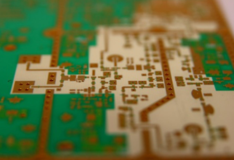
Printed circuit boards with high frequencies are much like any other form of PCB (printed circuit board). It supports microwave radio frequency communications, ranging from five hundred megahertz to two gigahertz. As a result of its ability to carry signals over longer distances, it is used in a wide range of devices, including radar, industrial, military, and medical equipment.
High Frequency PCB is a form of PCB where the printed circuit boards have higher electromagnetic frequency, often used in applications that require the transfer of specific signals between two objects. It can operate between 500 MHz and 2 GHz, making it an excellent choice for mobile, microwave, RF, and other high-speed design applications. A frequency above 1GHz is considered high frequency.
In addition to the electronics industry, many sectors worldwide use products that have high frequency PCBs for the advantages they offer: moderately low cost, reusable, highly durable, compact size that allows for reduced waste, along with many other benefits. Plus, this kind of PCB offers a wide range of applications contributing to many products in various industries.
Some of the common uses of high frequency PCBs are:
- It is used to make a variety of military-related equipment.
- It is used to make various printed circuit board instruments for medical equipment.
- High frequency is used in various machinery and equipment in the industrial sector.
- Communications can be done using high frequency radar devices built with PCBs.
It is important to know that the signals are vulnerable to noise and come with a tighter impedance tolerance than conventional circuits. In addition, it is also necessary to know that this type of PCB requires more energy because it is always interrupted due to noise.
One of the materials designers often choose for high frequency PCBs is Rogers dielectric material because of its lower dielectric loss and lower signal loss. Plus, it is better suited for rapid-response prototyping applications than other materials and has lower circuit manufacturing costs.
It is also possible to use FR4 in various applications with the correct material layering. It is through the use of the same dielectric material that this method contributes to the improvement. A lower loss factor and a lower dielectric constant provide such properties and are not dependent on system temperature or frequency.
The most widely used material for the substrate is PRFE, which has a lower loss. Most designers usually pick a low-loss FR4 laminate or low-Dk PTFE laminate as high frequency PCB materials. However, low Dk values are less important when creating homogeneity, and a high-Dk laminate or a standard laminate, or a high-Dk laminate can work just fine for your specific application.
Below is a detailed explanation of the properties of the high frequency materials that should be used in high frequency PCBs.
Start With High Frequency PCB Material Properties
The designer must consider that special materials are required for a high frequency PCB, providing high-speed signals. The dielectric constant and dissipation factor, along with other factors of the selected materials, play an important role, and therefore a prior analysis must be carried out.
There are specific high frequency PCB material requirements for constructing high frequency boards since a change in permittivity can impact the impedance of the PCBs:
- The permittivity of the material used must be adapted to meet the needs of the application.
- Signal transmission is made possible by reduced attenuation.
- Low Dielectric constant and insulation thickness tolerances for homogenous construction
Below are some of the material properties designers must focus on when selecting materials for high frequency PCBs:
Dk and Df
A low dielectric constant (Dk) and a low dielectric loss tangent (Df) are probably the first factors designers look for high frequency PCBs. When looking for the materials from suppliers, you'll find these values at specific frequencies, depending on that material's target market. Most designers are interested in this information as they usually need materials with low losses because their system needs that.
However, when designing high frequency PCBs, the values of these factors depend on the type of high frequency PCB you want to construct. But before we discuss that, let's understand Dk and Df values!
A dielectric constant (Dk) refers to an insulating material's capacity to store electric charges through dielectric polarization that hinders signal propagation. As a result, a delay in signals happens, which must not exist in a high frequency board.
Dk is a directional property of a material which means it changes with the change in the axis of the material. Therefore, the smaller the Dk value, the better the input stability, minimizing delay in signal transmission.
The dielectric loss tangent (tan δ) or the dissipation factor (Df) is another component based on the molecule's structure that can affect the RF material at high frequencies. It represents the energy absorption rate on an electromagnetic field when it passes through a material. In other words, it indicates a dielectric material's dissipation of electrical energy as a result of the different physical processes.
If the amount of energy absorbed by a dielectric material increases when traversed by high frequency signals, it results in signal loss as the molecules start to vibrate at a higher rate.
Thus, designers prefer small and stable DK and DF values for high frequency PCBs. Generally, the smaller, the better. A high Dk value may cause signal transmission delay, while a smaller DF can reduce the signal loss accordingly.
In high frequency PCBs, the type of the board you're designing determines the Dk value:
- For a small high frequency printed circuit, a larger real part of the Dk is required
- To achieve low loss, go for a low Dk imaginary component
A small Dk value is preferred when interconnects are very long and subject to a risk of excessive loss. Although Dk is unrelated to the dielectric losses when you set the impedance to your target value, it is important as it determines the operating signal's wavelength in a high frequency PCB. This also explains the need for larger Dk values for smaller circuits, which need smaller wavelengths.
Available Thickness and Panel Size
It might sound a little trivial, but high frequency PCB materials aren't always available in the thickness or panel size you want. These materials are usually copper-clad laminates of a specific thickness, several of which are stacked and joined by a layer of glue. They can also be stacked with other FR4 laminates having a similar thickness in a hybrid layup.
The board thickness and width of the circuit lines/copper traces are determined by the laminate thickness you can use to route high frequency signals and create high frequency circuits on a PCB.
Thus, the thickness of the board is the most crucial element as it determines the line width on which your system's target impedance depends. It is essential to consider when selecting high frequency PCB materials since developing impedance-regulated transmission lines is essential to avoid signal degradation. That's why all elements and components are designed for 50-ohm system impedance.
Microstrip and Stripline are two of the most commonly used techniques for creating impedance-regulated transmission lines. To be considered a microstrip, trace the top layer and a ground plane below.
You can calculate the impedance of a microstrip by considering the thickness and width of the trace variables, along with other factors, such as the relative permittivity of the board material and the height of the trace above the plane.
The thickness of the substrate still matters even if impedance-matching circuits are used to match the circuit board and system's impedance since thickness determines the distance from the ground plane layer to layer. Thus, to achieve smaller circuit sizes and line widths, you can use:
- thinner laminate for smaller circuits
- larger Dk value to get smaller circuits
The panel size is also an important detail, although less crucial than the thickness, as it determines the cost per unit. Purchasing from an outside manufacturer can be complicated since you are limited in the choice of material and can only draw from their inventory. Plus, they do not specify the panel size.
Types of High Frequency PCB Copper Foil
Now you know that the correct selection of materials in a high frequency circuit is essential since it will prevent them from sending mixed signals. It is important to know the characteristics of the materials because they can cause future problems. A clear example is the dielectric materials that count molecules that vibrate by the magnetic fields generated by the signals. If you put a high frequency on this, it will have a high vibration which will cause lost energy. Similarly, other significant energy losses can be caused by copper conductors.
High Frequency materials sometimes use a certain set of copper sheets that can be rolled, annealed, or low-profile to reduce losses as much as possible. You can evaluate the approximate losses from a good datasheet defining the approximate roughness (normally the z-axis RMS roughness); The lower the RMS roughness, the smoother the copper foil.
A smoother copper foil generally ensures lower resistance losses at lower and extremely high frequencies and is more desirable for high frequency circuits.
It is the best from a loss perspective since it reduces impedance mismatch and helps smooth out skin effects. For small-sized PCBs with very short interconnects, your focus should be more on the Dk/Df values than the copper foil type. In contrast, when long interconnects or a frequency above 2.4GHz is involved, you must focus on the copper foil type that ensures lower resistance losses.
However, there are other criteria to consider, such as the plating material that can be responsible for creating higher roughness losses by introducing a rough interface into the copper layer. Two of the surface platings with almost no extra loss over bare copper are the immersion silver plating (iMAG) and the organic passivation (OSP).
Copper foil is a key conductive material in the roots of PCBs, and its performance is closely related to its surface treatment. Therefore, whether it is electrolytic or rolled copper foil, it must undergo surface treatment before making it into a copper-clad board.
The demand for copper foil is increasing, and the quality requirements for copper foil are also getting higher and higher. Considering this, advanced copper foil production and surface treatment technologies have given rise to different copper foil types ideal for printed circuit boards.
HVLP Copper Foil
Hyper very low profile (HVLP) copper foil has an ultra-low profile with good etch ability and high peel strength. Its microstructure makes it an excellent material for high frequency PCBs using low-coarsening technology. It has the best performance among the different copper foil types but is also manufactured at a higher cost.
The use of HVLP copper foil is now recommended in PCB manufacture to mitigate the insertion loss, reducing the skin effect. It is essential since the skin effect increases the copper resistance reducing the channel's cross-sectional area. The effective signal path length on a rough copper surface can be much longer than the trace length.
RTF Copper Foil
Reverse Treated Foil (RTF) is a copper foil roughened on both sides to varying degrees, strengthening both sides' peel strength, making the copper foil a good intermediate layer with good adhesion to bond to other materials. In PCB manufacturing, the treated side of the copper foil is attached to the dielectric material.
The different treatment levels on both sides make the base foil more adhesive for the dielectrics, making the rough layer's thinner side easier to etch. This is the main advantage of RTF. The treated side does not need any further chemical or mechanical treatment and is already rough enough to have good adhesion to the lamination resin.
HTE Copper Foil
A high-temperature and elongation (HTE) is electrodeposited copper foil with excellent high-temperature resistance and high elasticity. This type of copper foil complies with IPC-4562 Grade 3 specifications and does not oxidize or change color at high temperatures. Plus, it can be easily laminated with other materials due to its good elasticity.
This type of copper foil is roughened on one side, making it a good adhesive foil for other materials in PCB construction.
The table below provides a brief overview of the copper foil types and their roughness levels:
|
Copper Foil Type |
Roughness |
Description |
|
Electrodeposited |
Highest (above 1 um) |
A copper foil with a rougher surface on one side |
|
RTF |
Moderate (0.5 um to 1.5 um) |
A copper foil roughened on both sides using surface treatment to reduce roughness |
|
Rolled-annealed |
Low (0.25 to 0.5 um) |
A copper foil with a smoother, denser surface due to a rolling process |
|
Ultra-low profile |
Lowest (can be less than 0.3 um) |
A copper foil with the lowest profile with the use of additional treatments to reduce roughness |
High Frequency PCB Material Thermal and Mechanical Characteristics
Below are some of the high frequency PCB material characteristics to keep in mind when selecting an appropriate one for your project:
- The axis of the material determines how it behaves; therefore, when the axis is moved, the behavior varies. Therefore, the dielectric constant must be small enough to provide a constant input for signal transmission.
- Similarly, the dissipation factor (DF) should be low, as a large DF would degrade the quality of the transmission signal. As a result, there will be less signal waste.
- Crosstalk and skin effects are diminished with careful spacing. When a board begins to communicate with itself, it is said to experience "crosstalk," which refers to unwanted coupling with its components. The space between the trace and the plane should be as small as possible to avoid crosstalk.
- The trace resistance is directly related to the skin effect. When the plate's resistance increases, the temperature increases as a consequence. When designing a circuit, it's critical to ensure that the track length and width do not affect the board at high frequencies.
- Vias with a smaller diameter have lower conductivity, making them more suitable for use at higher frequencies. It is preferable to have higher peel strength, impact resistance, and heat resistance value over high frequency PCB
- The coefficient of thermal expansion (CTE) describes the impact of temperature on the size of a material. Due to the material's sensitivity to temperature, even a slight change significantly affects PCB drilling and assembly. The copper foil should have the same thermal expansion as the rest of the foil, as a variation in thermal expansion can cause the copper foil to separate if the temperature changes.
- The environment in which your device works is quite essential. Using your device in a laboratory or indoor environment will not cause any moisture issues. When your equipment is exposed to a humid environment, problems can arise. Therefore, the high frequency PCB material water absorption should be modest as a significant absorption factor can modify the DF and DK values of moisture.
In addition, a series of thermal management techniques are important for the correct design and manufacture of a high frequency PCB:
- Wider tracks: The use of wider copper tracks helps maximize heat dissipation. It is necessary to take special care that these tracks are not too wide since they can cause crosstalk in the future.
- Insulation and refrigeration: This is where heat sinks come into play, for those elements that generate more heat and cooling fans that can be left exposed to the air and used as cooling in closed places to allow hot air to dissipate effectively.
- Thermal pathways: The set of pathways over copper-filled areas allows for efficient management, allowing heat to dissipate into the air through said pathways. The greater the number of ways, the greater the dissipation.
How to Select Copper Foil for High Frequency PCB Design
Technological advancements in the PCB industry have led to the development of materials with the lowest possible signal loss for high frequency applications. As discussed above, losses distort signals and limit their propagation, creating an impedance deviation. Likewise, the type of copper used also matters, and the smoothest possible copper foils are the best when designing high frequency printed circuits.
We have already discussed the impact of copper roughness on losses and impedance deviation and the benefit of using smooth copper foil, but how smooth copper foil should be. How to select copper foil for high frequency PCB designs?
Copper foil is not something you can pair up with every laminate material. Therefore, you'll have to look at the materials sets offered by a laminate distributor or manufacturer. Although not every manufacturer provides different material sets to pair with different types of copper foils, many manufacturers do this.
The different copper foil types for PCB materials, including the RTFs, rolled-annealed, HVLP, etc., have varied roughness ranges that determine the type of copper foil you need in your PCB. Therefore, when selecting materials for your high frequency PCB, you must examine the board capabilities and compare them with the dielectric and copper options. However, as discussed above, standard FR4-grade materials can work just fine for moderate frequencies. Also, the type of copper does not matter in such a case.
If you have a performance target to hit and high-frequencies are involved, the type of copper makes a huge difference.
The skin effect changes the impedance of the transmission line at higher frequencies. And the extent to which impedance is modified depends on the copper roughness. Three primary mechanisms produce the losses with the interaction of high frequencies, and copper traces:
- The rougher the copper, the more the electric field flux and the dielectric losses since rougher copper limits field lines to a smaller volume.
- At mid-range frequencies, the impedance, as well as the resistive losses, will be larger.
- There will be a slight impedance discontinuity with increased impedance and, if not matched, increased reflections.
Loss Budget
The loss budget for your highest frequency interconnects is the first point to consider when selecting the copper for your high frequency PCB. It is possible to estimate your RF lines' loss budget well if you know your board's approximate size or link length. High Frequency PCB components must have two specifications to source and receive high frequency signals:
- transmitter output power
- receiver sensitivity
Both specifications are described in dBm or mW. Here's how you can find the loss budget:
Loss Budget (dB) = [T* Power (dBm)] - [R* Sensitivity (dBm)]
Using the above formula, you can find your lines' accepted loss per length.
A Process for Selecting Laminates and Copper
There's a simple process you must follow when comparing copper and dielectric materials to ensure you achieve your operating targets:
- Assess the surface layer vs. the internal layer. It involves planning out the route of the roughness-sensitive interconnects and their floorplanning with the major components.
- You must know the loss tangent required for the operating frequency you want.
- Once you get a material set with the accepted loss tangent, examine the available copper options. Look for your high frequency PCB design's accepted copper roughness and surface plating.
- A heavier copper has lower skin effect losses. Therefore, ensure the selected copper foil is available in the right weight.
Remember that although copper selection and plating are important factors in a high frequency PCB, the dielectric aspects should be considered first, as they are the determining factors of the PCB stackup. The selection of copper roughness and plating comes next based on the available laminate materials.
High Frequency PCB Materials Table
Some of the materials that can withstand high frequencies include:
- Rogers 4350B High Frequency
- Rogers RO3001
- Rogers RO3003
- A Taconic RF-35 ceramic.
- TLX for Taconic
- E-fiberglass ISOLA IS620
- ARLON 85N, among others.
At this point, engineers work to establish a production process considering critical process factors such as line width and dielectric gap to ensure a robust design that meets user needs and performs consistently and reliably in all conditions.
High Frequency PCB Materials Table |
||||||||
|
Material for high frequency boards |
Dk |
Loss Tangent or Df |
Tg Glass transition temperature |
CTE |
Electric Strength |
Surface Resistivity |
Thermal Conductivity |
Peel Strength |
|
@10GHz |
@10GHz |
°C |
ppm/°C |
KV/mm |
MΩ |
W/m*K |
N/mm |
|
|
Rogers 4350B |
3,5 |
0,0037 |
280° |
32 |
31 |
5,7 x 10^9 |
0,69 |
0,9 |
|
Rogers RO3001 |
2,3 |
0,0030 |
160° |
- |
98 |
1 x 10^9 |
0,22 |
2,1 |
|
Rogers RO3003 |
3,0 |
0,0013 |
- |
25 |
- |
1 x 10^7 |
0,50 |
2,2 |
|
Rogers RO3006 |
6,2 |
0,0020 |
- |
24 |
- |
1 x 10^5 |
0,79 |
1,2 |
|
Rogers RO3010 |
10 |
0,0022 |
- |
16 |
- |
1 x 10^5 |
0,95 |
1,6 |
|
Megtron6 |
3,6 |
0,004 |
185° |
45 |
- |
1 x 10^8 |
- |
0,8 |
|
Taconic TLX |
2,5 |
0,0019 |
- |
135 |
- |
1 x 10^7 |
0,19 |
2,1 |
|
Taconic TLC |
3,2 |
- |
- |
70 |
- |
1 x 10^7 |
0,24 |
2,1 |
|
Taconic RF-35 |
3,5** |
0,0018** |
315° |
64 |
- |
1,5 x 10^8 |
0,24 |
1,8 |
|
ARLON 85N |
4,2* |
0,0100* |
250° |
55 |
57 |
1,6 x 10^9 |
0,20 |
1,2 |
Selecting High Frequency PCB Materials for High Frequency Applications
So far, you must have realized the importance of the choice of appropriate materials for a target application in your high frequency PCB design. Where high frequency PCBs are the pillar of wireless networks, smartphones, and other high-tech gadgets, they also have applications in the medical, automotive, military, and other sectors. Since their design is quite complex, designers must follow some guidelines to mitigate the interference issues involving high frequency signals.
Most high frequency applications have thermal management issues. Regarding losses, when a signal power input circumfluence is used, a higher loss will produce more heat. The other is related to the frequency; the higher the frequency, the more heat is generated.
In addition, the increase in heat in any dielectric fabric will cause the change of DK, that is, the temperature coefficient of the dielectric constant (TCDk). When the loss change causes the circuit temperature change, the temperature change causes the DK change.
For this heat loss ratio, different types belong to different materials, and therefore, their characteristics must be considered for high frequency PCBs.
Circuits using a very low-loss material and a very smooth copper foil will have relatively low insertion loss. However, if the same circuit is still used with the same low-loss material, using highly rough copper instead of plain copper will significantly increase insertion loss.
The surface roughness of the copper foil will affect the conductor loss of the circuit. It should be noted that the loss-related surface roughness is the surface roughness of the copper foil at the CU-dielectric interface when it is a laminate.
Also, if the medium used in the circuit is thinner, the surface of the copper foil will come closer together. In this case, the surface roughness of the copper foil will have a greater effect on insertion loss than the relatively thick medium.
Thermal management is a common problem for high-power RF applications, so selecting low DF laminates and smooth copper foils is more advantageous. In addition, it is advisable to choose laminates with high thermal conductivity. High thermal conductivity will help to transfer heat from the circuit to the radiator effectively.
There are many reasons why the temperature increases with frequency. One of the reasons is that the DF of the material will increase with increasing frequency, leading to higher dielectric loss and, ultimately, increased insertion loss and heat. Another problem is that the conductor loss increases with frequency. The increase in conductor loss is almost because the skin depth decreases with increasing frequency. Also, as the frequency increases, the electric field becomes denser, and a given circuit region has a higher power density, increasing heat.
Lastly, the TCDk is mentioned many times. This ubiquitous feature of DK materials changes with temperature and is often neglected. The power amplifier circuit has 1/4 wavelength lines in the booster network design, which are very sensitive to DK jitter. When DK changes significantly, the 1/4 wavelength match will shift, resulting in a change in power amplifier efficiency, which is highly undesirable.
In summary, when selecting a high frequency material for high-power RF applications, the material should have low DF, relatively smooth copper foil, high thermal conductivity, and low TC and Dk. Many trade-offs are needed to account for the characteristics of these materials and end-use requirements. Therefore, when selecting materials for high frequency PCB applications, the designer should contact their supplier.
Final Words
For high frequency PCBs, you need trusted and experienced specialists, such as the Hemeixin PCB, a reference in the design and manufacture of high frequency PCBs. When selecting the materials for high frequency PCBs, the Hemeixin PCB specialists have the know-how and expertise.
To place an order for a high frequency PCB with low-loss and high frequency materials, call +86 (755) 2758 6529 or visit us now!


