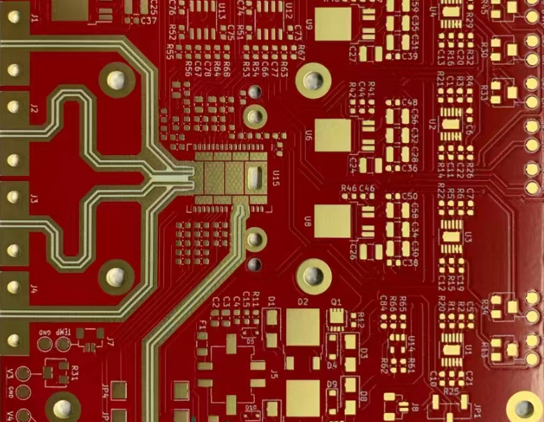
Getting Started With RF PCB Layout Guidelines
RF PCB layout is a different type of PCB that allows you to use radio frequency components along with digital and analog components in a PCB. As is the case for any PCB, there are certain proper guidelines you must follow when it comes to following the RF PCB layout in a PCB. PCBs are going through many improvements to ensure that they make creating circuits easier for engineers. Thus, as the technological advancement of these PCBs continues to grow, engineers also have to educate themselves on how to make these PCBs work for them.
PCB manufacturers have a special set of guidelines that, when you follow them, will allow you to create devices that were never possible before. However, these guidelines can be quite stringent and difficult to understand if you're unfamiliar with an RF PCB layout for PCBs.
The most important thing to recognize is that RF PCB layouts are different than a layout with digital and analog devices. Many PCBs can now use all three signals. However, you can use a PCB with an RF PCB layout to achieve the required circuit. An RF PCB layout is also much more prone to interference, which engineers can struggle with quite a bit when designing and constructing circuits.
In the article below, we'll list some major RF PCB layout guidelines to help you make better circuits moving forward.
What is an RF PCB layout?
An RF PCB layout or an RF design is similar to a mixed-signal PCB. However, with an RF PCB layout, you mostly cater to signals that how quite a high frequency or a radio frequency. An RF PCB layout PCB is unique because the PCB's substrate depends on any performance indicators requirements. The most common substrates are FR4 epoxy glass or a Teflon material.
There are certain standards that an RF PCB will follow:
- If the RF PCB works with low radio frequency, then the substrate will likely be a standard FR4 material. This type of material has effective insulation, stable materials, and a notable dielectric constant that adds to the overall effect of the RF PCB.
- It's also necessary for each component in this design to be arranged as close to each other as possible.
- If you're doubling the RF PCB layout with a mixed signal PCB, you must also ensure that the analog and digital partitions are separate from each other not to cause interference.
- When selecting components, you must pick as many SMD or surface-mounted devices as possible. SMD are generally quite small and have surface pins that can easily connect to the board.
The routing and layout of an RF PCB require you to be aware of certain parameters. Since the signals are generally high-frequency, you must follow these guidelines properly. It is necessary to consider a special kind of parameter system, including the amplitude and the phase shift the signal will go through, so signal reflections are kept to a minimum. Engineers must consider other major factors, such as the skin effect, electromagnetic interference, capacitive coupling between two major signals, and impedance control, which are still some of the major issues that electronic designers may undergo.
RF Concepts and Terminologies
Before we can get into RF PCB layout guidelines, you must understand certain RF concepts and terminologies. The major concepts that you must understand are as follows:
- Impedance Matching
- Characteristic Impedance
- Insertion Loss
- Return Loss
- Transmission Lines
One of the major factors that affect the RF PCB layout is the impedance of the RF circuit, which is why understanding Impedance matching is tantamount to establishing an RF PCB layout. At low frequencies, the impedance of the load doesn’t depend on the distance between the trace and the load. However, when considering a high frequency, the trace width and uniformity tend to alter the impedance of the overall circuit.
We use nodes to represent traces when measuring low-frequency signals. However, the load's impedance for higher frequencies will change as the distance changes. The impedance also depends on the substrate and the dimensions of the RF trace. Therefore, when we consider creating RF schematics, the trace is an important design element.
Transmission lines are a medium that creates paths for electromagnetic energy. Certain defined components make the best transmission lines, such as waveguides, coaxial cables, and RF traces. RF traces are generally made using the microstrip line and a coplanar waveguide. An RF PCB layout is made using RF traces.
Character impedance is also one of the most important properties of a transmission. It involves the ratio of voltages and currents of a wave that travels through a transmission line. An ideal transmission trace does not allow for any energy loss due to its character impedance. The character impedance is a strong property and depends on the type of material the PCB is made of, as well as the thickness of the substrate. Other factors that change the character impedance include the trace width, trace thickness, and the clearance of RF trace and ground fill. These parameters are exceptionally important in the RF PCB layout, and you must consider them accordingly.
Impedance Matching
Impedance matching is one of the first steps you will have to take when following an RF PCB layout for your PCB design. If a circuit doesn’t undergo impedance matching, it is much more prone to significant power losses. There are also problems, such as the reflection of harmful signals along the PCB traces. Impedance matching is necessary to ensure that the maximum amount of power can reach the load from the radio frequency component. If the impedance of the two components is not the same, they need to be matched so that the least amount of energy is lost.
When considering RF frequencies, the impedance measured can change as the distance of the loads changes from the RF component since RF is generally a higher frequency. Thus, as the impedance changes, you must change the network that the source and the load follow. If the impedance you measure matches the characteristic impedance, distance will not affect it. Thus, matching impedance is extremely necessary before designing the RF PCB layout.
The way to conduct impedance matching is to use a matching network near the source to match the character impedance of the source. Similarly, a matching network near the load will match the character impedance of the load so that the two nodes have the same impedance. Doing so ensures that the component values will stay the same as long as the matching networks are kept similar to the source and the load. The preferred components for impedance matching are inductors or capacitors. You could also use RF stubs, which take up much more space on the PCB.
RF Transmission Lines
Most RF components require the RF PCB layout to be in a way that allows maximum power transfer. The power transfer thus happens using transmission lines. These transmission lines can occur on the exterior parts of the PCB, top or bottom. They can also be placed in an internal layer somewhere. The guidelines for these transmission lines include further discussions about components such as the microstrip, the coplanar waveguide, the suspended stripline, and the characteristic impedance. You must also know a bit about the bends in the transmission line and the corner and layer changes.
There are several different types of transmission lines on the PCB. However, the most popular ones include the following:
- The Microstrip Line
- Coplanar Waveguide
Both trace lines are very different from each other. However, they follow the same purpose of providing transmission. These transmission lines are quite popular because they are cost-effective, simple, and have a lot of tools and information surrounding them. In PCB designs, the RF trace that transmission lines follow must be 50 Ohms.
Microstrip Line
It is a fixed-width metal trace with a ground space directly below, which creates this kind of transmission line. The ground plane, which is below, must be unbroken for maximum efficiency. If a microstrip is on the top layer, it will require a solid ground plane later on the layer below. The character impedance of the microstrip line is affected by four major features: the thickness of the dielectric material, substrate height, width of the trace, and the material's dielectric constant.
Suspended Stripline
With the suspended stripline, the routing is fixed width on the inner layer. There are also solid ground planes above and below the conductor for maximum effect. The conductor must also be midway between the ground planes, or it can be offset—the appropriate method for RF routing on inner layers.
Coplanar Waveguide
A coplanar waveguide is a component that is similar to a microstrip. But there is a copper filling on both sides beside the RF trace. This waveguide also provides better isolation between the RF traces due to the filling present. The factors that affect the coplanar waveguide are as follows: the substrate height, the width of the trace, RF trace thickness, the dielectric constant, and the gap between the trace and the copper filling. There are also return currents in the top layer, which are provided a direction through the layer into the ground layer underneath.
You may prefer the Coplanar Waveguide to the microstrip for many reasons. These reasons include the following:
- CPWG provides better isolation in the RF traces.
- There are also better EMI performances.
- Shunt elements that occur on RF traces are easy to ground
- Almost negligible crosstalk or crosstalk that is reduced immensely.
- The circuit has very less loss of energy for higher frequencies when we use a coplanar waveguide.
Characteristic Impedance
We have discussed impedance matching in the article before, and characteristic impedance may be similar. Characteristic impedance is necessary to set the correct impedance for your PCB for RF PCB layout. If you want to select the correct signal conductor line width to get the appropriate impedance, then you must use the correct characteristic impedance through calculation. However, with calculation, one of the things that you must be careful of is the presence of the dielectric constant. The layers will all have a different dielectric constant, and it's necessary to consider these values when calculating the required impedance. The external layers are laminated, and the dielectric constant is lower due to their decreased glass content.
Bends and Corners in Transmission Lines
We must also take care of the bends and corners in transmission lines when routing the RF PCB layout. In this case, you will have to use a bend radius at least 3 times greater than the center conductor width.
Doing this will help you reduce any characteristic impedance due to the bend. If a gradually curved bend is not working out for you, then a strict right-angle bend will also get you where you need to. However, with a right-angled bend, you will have to make some compensation as there will be some impedance discontinuity. One way you compensate is through a right-angle miter, a formula for compensation.
You can also use these compensation methods for other transmission lines. The bend can be created using an electromagnetic simulator if unsure about the right compensation. It allows for the creation high-performance transmission lines that make operations much smoother.
Changing Layers In Transmission Lines
The RF PCB layout can sometimes require layer changes so that the entire layout may fit. Here, if the transmission layer must move to a second layer, you would have to use two via holes for each transition so that some of the inductance loadings can be curved. When two vias are inserted, you will see a noticeable decrease in transition inductance by 50%. It is necessary to ensure that you apply the largest diameter, which is compatible with the width of the transmission line. If we take the example of a 15 mm microstrip, its diameter will be anywhere from 15 mm to 18 mm. If there are issues with space and this diameter of the via cannot be applied, then we will move on to three vias that use a much smaller diameter.
Guidelines for RF PCB layout Circuits
Now that we know a fair about the major guidelines engineers must follow when deciding on an RF PCB layout. We can further expand topics that are important to RF PCB layout guidelines.
RF circuit boards are quite sensitive to interference since they are not just using analog or digital signals; they also have RF signals. They demand much higher tolerances when designing circuits. The major aspects you must control in the circuit include reflections, noise, and ringing. The impedance from these aspects must be accounted for. As we have mentioned before, it’s important to route signal return current paths so they don't add to the additional noise. If you don't place a designated path for that particular current, then chances are that it will take the short path, which can cause issues.
It's necessary to be aware of the RF PCB layout to do your absolute best to bring about the best circuit simulation and analysis. If there are any problematic areas, you can find them and correct them too. However, as you know all the rules, you must take care of them. It's also necessary to understand that you will be required to deviate from some of the standard PCB rules to have the best RF PCB layout for your PCBs.
You must also ensure that you only deviate from these rules to maintain the Design For Manufacturing rules and achieve the best possible results through assembly and construction with limited errors. When designing an RF PCB layout, there are certain considerations that you have to keep at the forefront so you can achieve the best performance ever.
Component Placement for RF PCB layout PCBs
When you are placing components in an RF PCB layout PCB, there are certain things that you must take care of immensely. You must ensure that the part placement is much closer or tighter together. Managing the placement of components is essential as it ensures that the board follows the right standards for assembly so that you can keep the construction costs of the circuits to a minimum.
Many times, you may also be tempted to place the components on the metallic area of the RF boards as they allow for better conductivity near the external layers. However, this placement needs to be fixed, as it can create problems for the PCB assembly.
Another notion to keep in mind is that RF PCBs will require you to change the layouts and further alterations for maximum efficiency. The changes could be different sizes and shapes in the PCB. You could also change the size of the footprint pads so that you have better cushioning. Many people also add metallic features to increase the overall conductivity of the PCB. You may also want to note work of this kind can only happen on a component level rather than when you’re arranging the board or circuit design. There are also other adjustments that you can make on the RF PCB layout PCBs, such as trace routing.
Trace Routing for RF PCB layout PCBs
RF PCB layout PCBs also have routing requirements since we use high-speed and high-frequency signals. High-Speed and short, direct routing is essential for properly maintaining impedance in RF PCB layout PCBs. Impedance must be controlled when you have higher-current traces. Other trace routing rules to keep in mind can be the following:
- You must add the trace routing manually for specific RF technologies
- You must set up a functional design and make sure it works so that you can create a feedback loop. This act is necessary to set up a successful design.
- Use the function of copy and paste when designing the circuit on your computer. If there are similar circuits, then replication gets easier.
- To reduce impedance fluctuations, you can use curved or mitered trace corners.
- Vias also help protect areas of the ground plane for shielding.
With certain RF designs, you can use certain areas of the PCB as complete components, as it simplifies the design. However, this kind of routing will require special tools for parametric component routing. This routing is sent to the grouped components' trace segments and can undergo RF analysis.
There are also power and ground plane creation requirements that you can follow for trace routing. For these planes, you must create RF PCB layout designs with thermal relief that can handle different high-speed currents even through automated soldering. There are certain copper pours and planes in an RF PCB layout that a designer can sometimes convert to lumped components when running RF analysis. You may also have to use metal areas that have irregular shapes to create RF components. These elements can be created using CAD tools which engineers can further embellish to make intelligent group elements.
RF PCB layouts thus can use circuit boards in quite novel and innovative ways.
Other Guidelines for RF PCB layouts
Isolating Signal Lines
You must be careful when laying down a signal line, as interruptions or coupling can cause many noise issues. These are some of the preventative measures that you can take.
With transmission lines in an RF PCB layout, you want to ensure that you keep them as far away from each other as possible. It would be best if you did not route them close to each other for wide distances. If the microstrip lines are running close to each other in a parallel fashion, then the chances of coupling or noise increase the closer they are. Increasing parallel routing distance will also increase the coupling possibility. If lines cross each other on separate layers, there should be a ground plane that keeps them apart. High-power signal lines should also be kept at a distance from any other lines whenever possible. The reason for using a grounded coplanar waveguide is that there is extreme isolation between the lines when we use this. For small PCBs, you can reach an isolation of upto ~45 DB.
With high-speed digital signal lines, we follow a route separated by a layer to the RF transmission lines. This action stops coupling. The reason behind doing this is that you can easily prevent digital noise from leaking into the RF PCB layout circuit. Digital noise can couple with the RF signal lines and then shift to the RF components and carriers, leading to a much more complicated circuit. However, there are also chances of the digital noise being up/down-converted.
For power lines, routing occurs on a single dedicated layer. Providing the right decoupling and bypass capacitors for the Vcc node and the Vcc branches is necessary. It's necessary to choose the bypass capacitances while paying heed to a radio frequency integrated circuit and the frequency distribution nature that may arise from clocks or the PLLs. You should also ensure that these power lines are separate from any RF lines used to transmit higher power.
Ground Plane Considerations
A ground plane is one of the most important things to establish in an RF PCB layout PCB. Ground planes decide what paths your signals may want to head down. Experts recommend that you have a solid continuous ground layer as the second layer if you have kept the first layer for transmission lines and the other RF components. When adding the offset strip lines and standard strip lines, it’s necessary to have the ground planes be below and above the middle conductor. These planes must not have any assignment to the signal or power line but must have a direct connection to the ground to be termed ground planes. Due to some design restraints, you may have to create a local or partial ground region on one of the layers. However, you should ensure that this ground or partial ground is always underneath the RF components and transmission lines. You should also ensure that the ground plane doesn't break up any transmission routing.
Many layers likely separate the RF area, and between the layers, you must ensure that you add ground vias for maximum efficiency. The increased number of ground vias ensures that you can reduce the ground inductance from leaking through, as it reduces the number of ground current loops that may transpire. These vias also prevent cross-coupling between the RF paths and the other signal lines on the PCB.
Required Considerations for the Power and Ground Planes
The power and ground planes are the most important planes running the operations. When looking at the system bias/ power and ground layers, you must take care of any return currents. Experts recommend that you don’t try to route any signal in layers that run between the power or bias layer and the ground layer.
DC Decoupling and Power Traces
If your RF components have many power connections, it's necessary to pick one connection that is preferred over all the others. Establishing this star route simplifies the connectivity of RF PCB layout PCBs. To create this route, you have to place a large decoupling capacitor as the root of the star and then couple them with other smaller capacitors as the branches of the star. The Radio Frequency IC will determine the frequency range these smaller capacitors work at and how they function.
The advantage of this route is that it's short and takes up less space. Longer ground paths can cause a lot of parasitic inductance, which you can avoid using the star route in an RF PCB layout. One major consideration in DC decoupling is defining the DC supply connection with an AC ground.
How to Select Decoupling or Bypass Conductors?
Now that we know how necessary it is to apply Bypass Conductors, we can talk about their selection. Regular capacitors have a very limited frequency range since they have a self-resonant frequency or SRF. This SRF is not something that you can change. Rather, it comes from the manufacturer and may be much clearer when measured directly. Beyond the SRF value, the capacitor will turn into a conductor and cannot offer to decouple.
To conduct broadband decoupling, you must use several other capacitors of growing sizes so that they are all connected in parallel as per their requirement. The higher the SRF, the smaller will be the capacitor value.
Layout Considerations for a Bypass Capacitor
The supply lines must have an AC ground, so you must reduce the parasitic inductance that you add to the AC ground return path. The parasitic inductance may occur due to any layout or component orientation choice, such as that of the Bypass Capacitor's ground. There are two major methods that you can do so:
The first involves connecting the vias from the Vcc top layer to the inner power plane, which can generally resist the ground return and create a longer path with much higher parasitic inductance. This action will cause an AC that may encounter the Vcc pin to go through the bypass capacitor on the ground side before it gets back to the inner ground layer. This path allows for the smallest possible path for the capacitor and the vias.
On the second path, you will not stop the AC ground return paths using the power plane vias, and this kind of configuration requires more PCB area.
Grounding for Shunt- Components
The recommended practice for shunt-connected components is to use two grounding vias for each component. Doing so can severely limit the effects of parasitic inductance, which are necessary for RF PCB layout designs.
A Ground Area for IC
ICs or Integrated Circuits require a solid ground space underneath a component on the same layer. The radio frequency and direct current flow are generally carried to the PCB through this designated area for maximum efficiency. The other purpose of this ground pad is to act as a place where heat can dissipate. Hence this pad should have as many vias as possible. All of these vias must have some coating, and you may even fill them with a thermal paste for better thermal performance.
Final Thoughts
The RF PCB layout is one of the most complicated layouts out there, but there are certain actions that you can engage in to ensure that you have the best-designed circuit when using RF components. The most important actions you will engage in involve inductance matching, as your purpose for these RF PCB layout PCBs is to limit the power loss. You must also establish a ground plate and a power plate so the current knows where it must flow.
Trace routing, creation of signal lines, and routing lines are also important factors that you must be aware of before starting your RF PCB layout circuit if you want to avoid both impedance and noise.
If you want to know more about RF PCB layout guidelines, you will be happy to know that we deal with the best RF PCB layout PCBs to provide quality services and PCB manufacturing. Visit our website to learn more about the guidelines for flex, rigid-flex PCBs, and RF PCB layout PCBs.


