What is a Mixed-Signal PCB?
If you're looking for all the potential components that you may need to study electronics or engineering, then a mixed signal PCB is something you may have come across. Mixed-signal PCBs sound pretty complicated, but the idea is relatively simple. If you know anything about computers, you will know they have analog or digital input. You can work with both analog and digital signals in a mixed-signal PCB.
However, the mixed-signal PCB requires a fair bit of knowledge before you can start working on it. A mixed-signal PCB is a printed circuit board, and you can generally receive both signals here. However, you must follow certain rules and guidelines to ensure there's no signal interference. In the article below, we'll be looking at the components that make a mixed-signal PCB and what you must do to ensure that you meet the correct requirements to make this kind of PCB work for you.
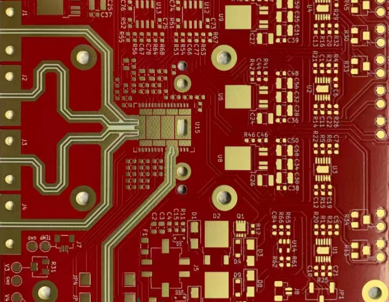
Mixed-Signal PCB
If you've come thus far, you're likely trying to answer the question of what a mixed-signal PCB is. We can break it down into two words: mixed signal and PCB. Mixed-signal means involving more than one signal. The signals that a PCB can receive are either analog or digital; similarly, those are the two signals that a mixed-signal PCB can accommodate at the same time.
In a mixed-signal PCB, you will have a printed circuit board with both analog circuits and digital circuits that can fit on the same board. If you think about it, there are applications of this sort everywhere in the world. One of the most common applications is that of a smartphone.
Once you know what the mixed signal stands for, you can look at the other part of the definition, the PCB. A PCB is a printed circuit board that you can use to assemble different components per your requirement. Most printed circuit boards are used as a vessel to receive analog and digital signals.
An analog signal refers to a continuous signal like audio and temporal signals, whereas digital signals are discrete and occur in zeros and ones. Mixed-Signal PCBs can handle both.
Is Understanding Analog and Digital Systems Important?
When working with a mixed-signal PCB, you must understand how the analog and digital signals systems work. You can’t expect to prevent all signal interference, but for the most part, you can try to keep it at bay. When considering the working of modern systems, an understanding of both digital and analog systems is necessary. You must also know enough to ensure that the integrity of both these systems is maintained.
The major factor that you must understand when it comes to mixed-signal PCBs is that there are some processes that you must undertake to ensure that signal integrity is maintained. These processes include component placement, net routing, and power and ground planning. There are also other factors that you may have to consider when constructing and using a mixed-signal PCB.
Two Main Types of Signals
A mixed-signal PCB uses both analog and digital signals. If you’re not familiar with analog signals, you may want to get familiar with them now.
Analog Signals
Analog signals are all around us, and in the simplest form, they occur continuously. What could mixed-signal PCBs use analog signals for? Well, the answer is simple. You can use circuits to measure values like force, sound, or even temperature. Analog signals are much more common for real-life applications, so it's necessary to know as much as possible about these and how they are translated into digital signals. Sometimes, the circuit must convert a digital signal to an analog signal so the circuit can run a motor. Understanding how these analog signals work helps you further understand the distinctions you must make while assembling a mixed-signal PCB. These signals are also expected to be limited in noise or pure, which is why there are so many restrictions when using a PCB of this sort.
Digital Signals
A digital signal is also one that a mixed-signal PCB can take as input. It’s also important to distinguish that mixed signal PCBs often read low-speed digital signals; thus, low-speed digital signals are also something you must be aware of.
A digital signal is simply a series of bits or 1s and 0s. It has discrete levels, unlike continuous analog signals that seldom occur in levels. Low-speed digital is defined by the boundary that we place on them. A low-speed digital signal could mean anything less than 20 MHz if that's the consideration we're currently making. However, for the construction of a mixed-signals PCB, it’s enough to know what these digital signals are and how they are often used in combination with analog signals.
Digital signals are often used with actuators when something needs to be controlled. They are also often used with integrated circuits, which is why mixed-signals PCBs also allow for the use of these signals.
Guidelines for Mixed-Signal Printed Circuit Boards
If you need more clarification about the factors you must consider before starting work with your mixed-signal PCB, you may not be the only one. Electronics have come quite a way in the past two decades. We used to have multiple circuit boards that used to handle different aspects of the circuit, but now circuit boards are much more advanced. The mixed-signal PCB is one such PCB that can handle two different types of signals. However, with this kind of PCB, you must maintain some considerations to ensure that the circuit works as you require it to.
Understanding the layout of your mixed-signal PCB is essential to attach the components as you want. We’ll explain the considerations and layout of a PCB to you.
1. Component Layout in Mixed-signal PCBs
Think about building your circuit like a house; you must clear a proper floor plan to know where everything will go. You also want to avoid different aspects of your house interfering with each other, so you must be careful with the planning. A circuit on a mixed-signal PCB is the same way. You want to maintain the design and structural integrity of the entire circuit so that it works seamlessly. For this, you must follow the correct component placement design.
There are many ways to create a proper floor plan, but many engineers prefer using CAD software so that all the plans are in digital form and can be referenced frequently. The first step is ensuring that your mixed-signal PCB is partitioned so there are no signals intermingling and that the overall operation of your circuit is smooth. The signal integrity can get compromised if there are problems such as EMI and crosstalk. We'll talk about partitioning later in the article, but for now, you should know that it's an important step for functioning a mixed-signal PCB. Other major considerations when you place components are as follows:
2. Stick to the Partitions
Most analog and digital components are extremely sensitive, and keeping them apart from each other is one of the most necessary things you must do otherwise, your circuit can get extremely complicated. You may be tempted to stray away from the floor plan as you progress into making your circuit. However, with a mixed-signal PCB, you must keep the components separate.
3. Know the Components that You Must Place in the Center
The larger components like the processor and the memory, are ones that you should keep in the center. These larger components generate a lot of heat and release more heat than the rest. The major components are best placed in the center to ensure that the thermal dissipation doesn't harm your circuit.
4. Use of Bypass Capacitors
If there are any grounding issues or power fluctuations, then the power integrity in your mixed-signal PCB can change drastically. Integrity is essential in ensuring that all systems work to the best of their capability. To ensure that the power integrity doesn't shift around too much, bypass capacitors must be able to counteract some fluctuations. Mixed-signal PCBs require both direct and short routing, so bypass capacitors need to be placed as close as possible to the assigned pins.
5. Routings and their Associations
The schematic you build must have the appropriate signals for both the processor and the memory components. You must begin with the connectors and lay every other part around the processor and memory so that the signal integrity is not compromised. The signal paths must be complete and issue-free, so the circuit can work as required when you’re using a mixed-signal PCB.
6. Power Supply
A power supply is essential to the working of your circuit regardless of the kind of PCB you use. In a mixed-signal PCB, you must completely isolate the circuitry of each power supply from the digital and the analog circuitry for it to function. However, the catch is that the supply must also be close enough to the devices they are powering. Furthermore, each power supply must also have enough space between each other so that the thermal capacity of the mixed-signal PCB isn’t overpowered. For the best power integrity to be followed, the components must be as close as possible to the power supply from which they are extracting power.
If your mixed-signal PCB is supposed to deliver power, then that’s also something you must account for in the overall design of the PCB.
2. Partitioning
A major aspect you must follow in mixed-signal PCBs is appropriate partitioning. Noise problems frequently arise in mixed-signal PCBs, and partitioning ensures that you can keep this issue at bay. Partitioning is all about placement considerations; thus, it works in combination with component placement. Routing and thermal compensations must be managed when partitioning to minimize signal interference.
The major focus of partitioning is to ensure that the analog and digital circuitry don’t leak into one another and create crosstalk. You may question whether there should be separate or split ground planes for the analog and digital circuitry. For high-voltage current-carrying circuits and analog and digital signals completely separate from each other, separate ground planes are the best mode of action to proceed with. However, this action can also lead to new EMI problems you wouldn't have to face when keeping ground on one plane.
You must follow some considerations when it comes to partitioning analog and digital planes. We have mentioned them below:
- Keep sensitive analog devices like voltage references and amplifiers on the analog plane. Similarly, you also want to keep the digital components that create the greatest amount of noise, like the timing block on the digital plane, so they don't create interference. Having this divide ensures that leakage is minimum.
- Suppose your circuit or system has any mixed-signal analog-to-digital converter components or even digital-to-analog converter components. In that case, you may want to group these components into the analog plane of your mixed-signal PCB for maximum efficiency.
- If the design is complicated, you want to ensure that the supplies are split evenly. It means that if you have more than one ADC or DAC, the analog plane should have its voltage supply and the digital plane its own.
- Both microprocessors and microcontrollers are large components that create heavy bouts of heat. You want to place these components in the center to distribute the heat evenly.
3. Power Supply Monitoring with Decoupling Techniques
One major feature you must contend with when designing a circuit on a mixed-signal PCB is the Power Supply Rejection Ratio (PSRR). When designing a circuit, this is one of the most crucial aspects you want to take care of. PSRR measures how sensitive the circuit is to variations in the power supply. The fluctuations determine how well the circuit performs; thus, the PSRR is a significant measure.
To ensure that you have the best PSRR possible, you want to detract the high-frequency signals from entering the device. Decoupling allows you to find ways to restrict such high-frequency signals. All you need to do is set up capacitors in a way that allows you to decouple the power supply to the low-impedance ground plane.
Decoupling allows you to maintain a low-noise environment which is essential to maintain, especially in a mixed-signal PCB. The idea is to give the current a simple route by providing the most direct path forward. Correct decoupling techniques and implementation can help with a better power supply rejection ratio or PSSR. Some of the guidelines to follow when monitoring a power supply in the mixed-signal PCB is as follows:
- To minimize low-frequency noise, electrolytic capacitors act as the best reservoirs for transient currents in the power supply. However, opting for low-inductance ceramic capacitors is recommended to minimize high-frequency noise. There are also ferrous beads that can help eliminate any spikes of high-frequency noise.
- For the most effective use, you must place decoupling capacitors close to the device's power supply pins. You can also limit any additional series inductance by using a short trace to connect a large area with a low-impedance ground plane.
- Place smaller capacitors like 0.01 μF to 0.1 μF as physically close to power pins as possible to limit any instabilities when several outputs switch simultaneously. Larger electrolytic capacitors should remain only one inch away from the power pin of the device.
- If you don't want to create a trace, you can connect the decoupling capacitors to the ground using T-type connections near the GND pin of the device.
4. Grounding
If you’ve ever set up a circuit, you likely know how essential a ground plane is. A ground plane provides a signal return path within the design and can split or separate. With mixed-signal PCBs, a ground plane is even more important as both analog and digital circuitries must be separate. If you employ a separate ground plane, there can be greater issues as the return paths can become fractured. If you opt for separate ground, the signals may have a more complex return path, meaning they would have to find an alternate through the shielding, cables, or the frame. Such action is less than ideal as it creates a lot of additional noise that can harm the integrity of your circuit.
When working with a mixed-signal PCB, the best course of action is to use a single unit ground that is neither split nor separate, as it can act as a reference plane. If you’ve conducted the partitioning properly, the mixed-signal PCB is backed up with the technology that allows for return paths for signals to be seamless. The circuitry speed is quite fast nowadays, so the return paths can remain as close to the outbound signal routing given that the return path remains unbroken. You must also ensure that nothing comes in the way of the return paths or the ground.
Clear return paths are one of the major advantages of the single-plane ground. However, there are also some other major advantages:
- The circuit’s sensitive circuitry remains majorly shielded from the incoming EMI.
- Single planes will protect your sensitive circuitry if there is any other major internal interference in the circuitry.
- The larger plane allows you to take advantage of the lower impedance.
- The larger plane also ensures that the heat is properly dispersed across the board.
You may still opt to split the panes. However, power becomes a major issue in such a case. You must ensure that splitting doesn’t harm your pins’ connection to the power supply.
Analog and Digital Ground Separation
Analog and digital mixed-signal PCBs are more challenging when finding a single solid ground scheme. A split-ground plane is popular when it comes to such a circuit. The split is pretty simple. You have the analog and digital ground planes, and they are kept from each other.
With systems such as these, to be more cohesive, you may want to remove any obstruction between the two so that the currents can take a simple track through the junction between the analog and the digital planes. Mixed-signal PCBs will generally follow such a design if the circuit is too complicated for a single one.
A star ground could be a common ground that both analog and digital signals can follow. It often connects the analog ground to the digital ground. As a designer, you must look at the datasheet for each component to ensure the grounding specifications for each component are met. If any devices have both AGND and DGND inlets, you can join these pins to the star ground to simplify matters for yourself.
Further Grounding Practices
You can follow some other grounding practices to ensure that all the devices in your circuit are grounded.
- Use wide copper traces to connect when joining the Star ground.
- Verify the board for any narrow traces; these aren't connections you want.
- Pads and vias can ensure that you can connect your analog and digital planes if necessary.
5. Trace Routing
Trace routing helps you understand the paths followed by the signals. If properly partitioning the PCB is done, trace routing becomes easier in a mixed-signal PCB. However, there are some factors that you may want to consider when it comes to tracing routing. We have mentioned some of these below:
- Make the paths as short and direct as possible so signals don’t intermingle.
- Ensure that you follow the signal paths as they appear in the schematic for high-speed circuits. Signal paths can become confusing, and it's necessary to stick to the given paths.
- Power supply traces must also be short and direct to minimize inductance.
- Be careful of antennas that may occur due to traces or vias
- You should maintain isolation in the routing between analog and digital.
- Grounding is of the utmost importance for any mixed-signal PCB circuit.
You must stick to the rules regarding trace routing because you must refrain from doing so to avoid having more issues. Follow trace routing software to map out the traces to a tee before assembling the circuit.
6. Copper Traces and Its Issues
Copper is the material that most of these mixed-signal boards are made of, and it’s not perfect. You must be careful when constructing a circuit because you must account for the fallacies of copper to create those connections. Copper has resistance, which can create issues as far as the layout of mixed-signal PCBs is concerned.
One thing to consider is the thickness of copper on these boards. Mostly, copper only has a thickness of 1 inch, but there are places where the thickness can increase to two or three inches. Resistance is an electrical property, and it is closely related to the area and length of the material, so when the cross-sectional area or the length increases, it will have an overall effect on the resistance of the circuit. If the resistance is too much, it may create issues with the circuit's thermal distribution.
When mixed-signal PCB resistance increases, it can increase the error frequency in the mixed-signals. If you’re managing a low-impedance precision circuit, then the increasing resistance of copper may create significant issues with the overall design.
Final Thoughts
Mixed-signal PCBs are of great use because they allow you to include analog and digital signals in one circuit. However, these mixed-signal PCBs can also be quite complicated if you're unfamiliar with them. We suggest that you familiarize yourself with both analog and digital signals and how you can apply them in a mixed-signal PCB.
You can follow guidelines to ensure that the circuits you follow for your mixed-signal PCB work. We have listed some major guidelines for partitioning and grounding for these systems, as they remain an essential part of working with these boards.
If you're not entirely sure how to design a circuit on a mixed-signal PCB or need further clarification on getting the components to build these circuits, you can visit our website to get more information today!


