What is PCB assembly with SMT process?
Printed Circuit Board Assembly Introduction
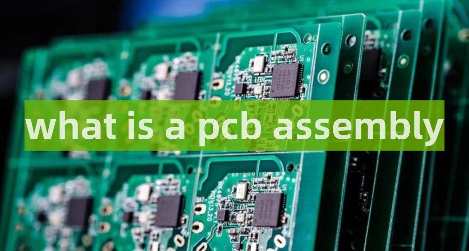
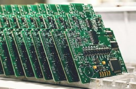
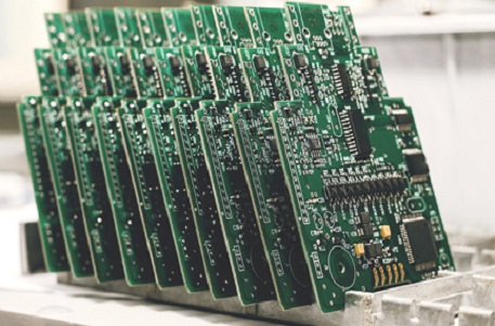
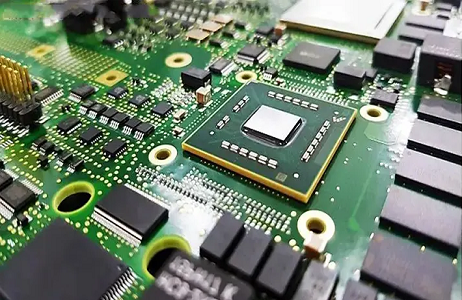
A printed circuit board assembly (PCBA) describes the finished board after all the components have been soldered and installed on a printed circuit board (PCB). The conductive pathways engraved in the laminated copper sheets of PCBs are used within a non-conductive substrate in order to form the assembly. Attaching the electronic components to the PCBs is the concluding action to create a fully operational electronic device.
What does a printed circuit board assembler do?
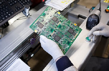
A circuit board assembler prepares printed circuit boards (PCBs) by soldering electronic components onto them. Reading wiring diagrams, following sample boards, selecting electrical components, and finishing the boards with hand tools are all part of this job.
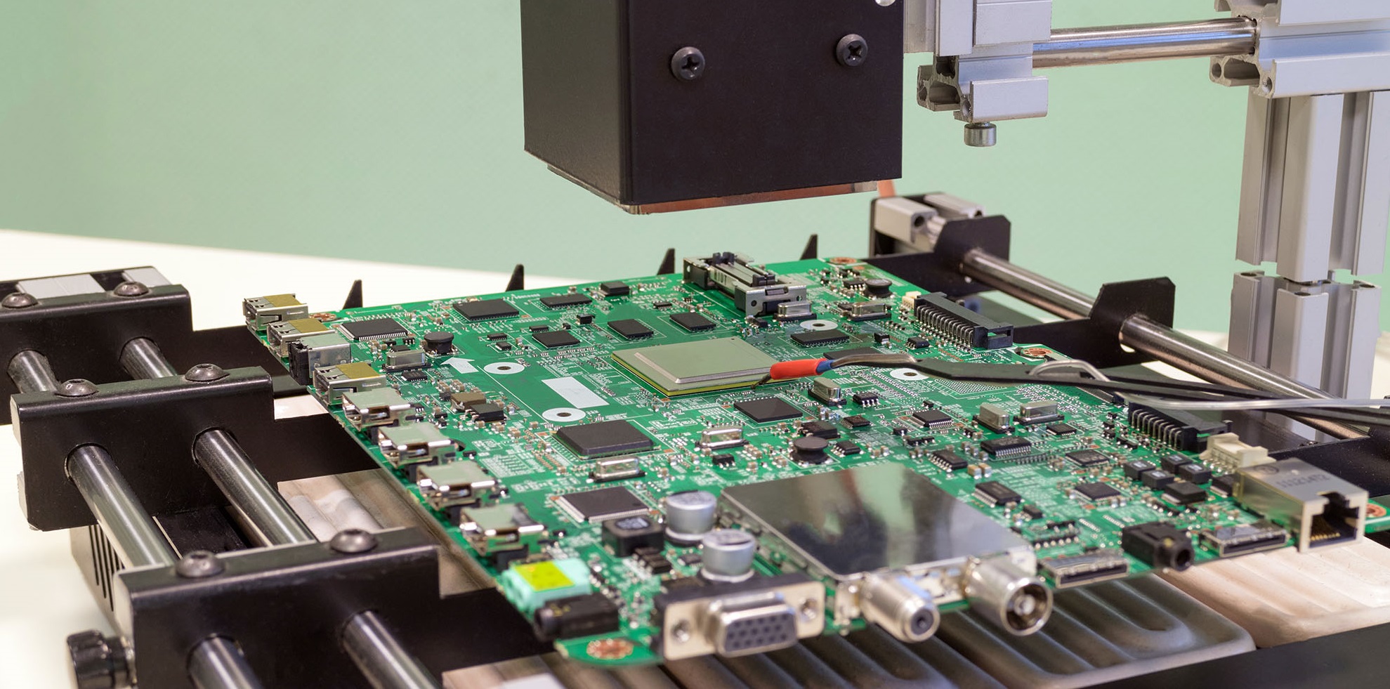
PCB Assembly Technologies
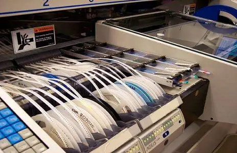
Assembling a printed circuit board requires more than just the raw components and a well-designed board. It also requires the right technology. In this case, there are several options to choose from, and each brings something different to the table. For instance, there’s surface mount technology (SMT), as well as manual soldering, and the use of pick and place machines.
While some PCB assembly processes will require just one technology, others will require a combination of two or more technologies. For example, many boards require the combination of through-hole technology (THT) and surface mount technology. Understanding when, where, and how to integrate those technologies is a critical consideration when choosing a company to handle your project or production.
It’s also important to understand that the PCB assembly steps involved with the various technologies differ, as well. Below, we’ve outlined some basic steps involved, as well as how they differ from technology to technology.
PCB Assembly Process
- Solder Paste: If you’re following a traditional PCB assembly process, the first step is the application of solder paste. Note that this is not the case with THT, but SMT does require paste application and/or printing.
- Component Placement: In the traditional PCB assembly process, the next step is to place the components on the board. This can be done manually, or it can be done with the assistance of machinery (pick and place systems). In THT assembly, components are placed by hand, which requires incredible precision. In the SMT process, robotic systems place components on the board. Note that automated placement is far faster than manual placement and is just as precise.
- Reflow: In the traditional PCB assembly process, the next step is reflow, which is when the solder is first melted and then resolidified. The board and all its components move through an oven, which heats the solder, liquifying it and ensuring that connections are formed before the board moves into a cooler, where the solder is cooled.
Note that the THT process does not require reflowing solder. Instead, the second step here is to inspect the board and rectify component placement. This is due to the manual placement process – a visual inspection in conjunction with a design transport frame helps ensure placement accuracy.
In the SMT process, reflow soldering takes place at this time, as well. The board is sent through a furnace, which melts the solder paste, allowing it to flow as necessary, before the board passes through a series of coolers that gradually bring the temperature down, solidifying the solder on the board and cementing the components in place.
- Inspection: The next step in the traditional PCB assembly process is a visual inspection of the board, soldering, and components. Note that this step has already occurred in the THT and SMT processes.
- Through-Hole Part Insertion: The traditional process requires that through-hole insertion be done manually, after the reflow and inspection process. Soldering is also often done manually, but it may be done using wave soldering.
Wave soldering occurs during the THT process at this point, as well. The entire board moves over liquid solder and then moves through coolers to solidify the solder.
Note that there is no correlating step in the SMT process (it is actually already finished, and wrapped up after just three steps, although a visual inspection should still be conducted to ensure accuracy and to reduce the potential for errors).
- Final Inspection and Cleaning: The final step in the traditional PCB assembly process is a final inspection of the board, the solder points, and the components, and a cleaning to ensure that debris or excess solder is removed.
PCB Assembly checklist
Hemeixin wants our customers to experience a seamless and accurate assembly process. To ensure that your job is not placed on hold, please follow these guidelines:
1. Accurate Data
An error free assembly process requires accurate data. Each job should have a BOM (bill of materials), a pick and place file (also known as a centroid file) and matching Gerber data. Add a DO NOT POPULATE (DNP) column to the BOM if there are parts which should not be populated on the PCB.
2. Ensure Proper Footprints
Some parts are available in different packages. Make sure that the part you specify in the BOM matches the footprint on the PCB.
3. Organize Components
Parts should be separated into individual bags or trays. Each bag or tray should be marked with Manufacturer name and Manufacturer part number and all reference designators where the part is used. If needed, you can substitute distributor name and part number in place of (or in addition to) manufacturer information.
4. Multiple Jobs Per Order
The parts for each job should be packaged separately. Include separate BOM and pick and place file for each job
5. Component Quantities
Include extra parts to account for possible attrition during assembly.
Extra parts will be required on small builds (1 to 25 boards) as follows:
- 0201 to 0603 size: Minimum extra quantity 50 plus required quantity.
- 0805 to 1206 size: Minimum extra quantity 25 plus required quantity.
- On large size components 1 or 2 extra parts is fine.
- We prefer all SMT parts to be on a continuous strip or reel.
- For large runs extra parts by percentage is OK
We will return any unused parts to you when we ship your assembled boards back to you.
6. Update your BOM and Pick and Place File
If you have any last-minute design changes, please remember to reflect these changes in your BOM, pick and place file and any other relevant documentation.
7. Mark Polarity
Make sure you indicate proper orientation for all parts that have polarity. Place a dot or a number “1” on pin 1 of ICs where the orientation is not obvious. Ensure that polarized capacitors and diodes are properly marked.
8. Special Instructions
Provide detailed instructions for any special procedures required to assemble your boards. Include sketches, photos, PDF files and/or drawings as needed
Choose components for your PCB Assembly
As a designer, you need to make some key decisions about the type of components used in your board. Stick to these guidelines while choosing parts for your board assembly.
1. Procure components from a reliable supplier
Sourcing all the components from a reputable manufacturer reduces the risk of counterfeit or damaged parts
2. Opt for IC packages to reduce the part count
Component packages integrate several parts into a single enclosure to perform a desired function. For instance, a basic filter circuit consists of aresistor and a capacitor. If you opt for a package that functions as a filter, you can minimize the number of components used on your board. This results in improved reliability, reduced weight, and cost of your board.
3. Select SMT components as much as possible
SMT components have shorter leads when compared to through-hole parts.This reduces the parasitic capacitance and enhances signal integrity. Otherbenefi ts of choosing SMDs are:
- Less maintenance
- Make boards smaller and lighter
- Placing SMT components on both sides of a PCB allows for moredesign fl exibility
- Easier to automate assembly compared to THT components
- Reduced manufacturing costs
Choose THT components only in special cases where the component requiredis not available and SMD is particularly sensitive to temperature.
Key takeaways:
1. Always procure components from a reliable supplier to avoid the risk of counterfeit parts
2. Implement component packages to reduce the part count and size of the board
3. Use small lead SMT components to enhance the signal integrity
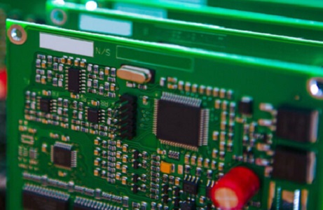
Differences between through-hole technology and surface mount technology
- SMT frees up the limitation on board space posed by the through-hole mounting manufacturing process.
- Through-hole components involve higher manufacturing costs than SMT components.
- You require advanced design and production skills for using SMT when compared to through-hole technology.
- SMT components can have a higher pin count as compared to through-hole components.
- Unlike through-hole technology, SMT enables assembly automation which is suitable for high production volumes at lower costs when compared to through-hole production.
- SMT components are more compact leading to higher component density as compared to through-hole mounting.
- While surface mount leads to lower production costs, capital investment for machinery is higher than needed for through-hole technology.
- Through-hole mounting is better suited to the production of large and bulky components that are subjected to periodic mechanical stresses or even high-voltage and high-power parts.
- SMT makes it easier to achieve higher circuit speeds because of its reduced size and fewer holes.
Guidelines for PCB Assembly component placement
Here are some recommendations for SMD placement to maintain good signal and power integrity for your board.
- Keep the components as near as possible to minimize the routing distance.
- Adhere to the signal path as per the schematic while placing the components.
- Never place the components in the return path of sensitive signals. This leads to signal integrity issues.
- For high-speed devices, place the bypass capacitors closer to their power pins. This will reduce parasitic inductance.
- Arrange the SMD together for power supply circuits. This will help you to provide shorter routing and reduce the inductance in he connections.
- Try to keep SMT components on one side of the board to reduce costs associated with stencils and assembly.
- Maintain the minimal spacing between the test points and SMT components as specified by your manufacturer. This spacing may vary depending on the component’s height.
To facilitate the assembly process ensure that all component names, polarities, orientations, and placements are marked properly in the assembly drawing. The footprints present in the drawings should match with the actual parts. Consult your manufacturer for their kitting guideline if you are considering consigned assembly. Prepare your BOM accordingly.
Before the PCB Assembly Process
A few preparatory steps have to happen before real PCBA process even begins. This helps PCB manufacturers assess the functionality of a PCB design, and primarily includes a DFM check.
Most companies specializing in PCB assembly need the design file of the PCB to start out, along with any other design notes and specific requirements. This is so the PCB assembly company can check the PCB file for any issues that may affect the PCB's functionality or manufacturability. This is a design for manufacturability check, or DFM check, for short.
The DFM check looks at all the design specifications of a PCB. Specifically, this check looks for any missing, redundant or potentially problematic features. Any of these issues may severely and negatively influence the functionality of the final project. For example, one common PCB design flaw is leaving too little spacing between PCB components. This can result in shorts and other malfunctions.
By identifying potential problems before manufacturing begins, DFM checks can cut manufacturing costs and eliminate unforeseen expenses. This is because these checks cut down on the number of scrapped boards. As part of our commitment to quality at a low cost, DFM checks come standard with every Hemeixin project order. Hemeixin provides FREE DFM and DFA check with, however, priceless values because Valor DFM/DFA check Hemeixin depends on is an automatic system contributing to high speed and accuracies.
After PCB Assembly
Suffice it to say, PCB assembly process can be a filthy one. Soldering paste leaves behind some amount of flux, while human handling can transfer oils and dirt from fingers and clothing to PCB surface. Once all is done, the results can look a little dingy, which is both an aesthetic and a practical issue.
After months of remaining on a PCB, flux residue starts to smell and feel sticky. It also becomes somewhat acidic, which can damage solder joints over time. Additionally, customer satisfaction tends to suffer when shipments of new PCBs are covered in residue and fingerprints. For these reasons, washing the product after finishing all the soldering steps is important.
A stainless-steel, high-pressure washing apparatus using deionized water is the best tool for removing residue from PCBs. Washing PCBs in deionized water poses no threat to the device. This is because it's the ions in regular water that do damage to a circuit, not the water itself. Deionized water, therefore, is harmless to PCBs as they undergo a wash cycle.
After washing, a quick drying cycle with compressed air leaves the finished PCBs ready for packaging and shipment.
PCB Assembly Services
Hemeixin is the premier PCB solutions provider. We can cover your PCB requirements from parts sourcing to electronic assembly. We'll help you with each step of the way and provide you with comprehensive expertise and quality assurance.
When you choose us as your cooperative PCBA company, you're choosing to partner with a service that delivers the best. Our PCB assembly services meet the highest quality benchmarks and follow IPC Class 3, RoHS and ISO 9001:2008-certificitation standards . Additionally, we can handle any kind of PCB, whether it's double-sided or single-sided, an SMT, through-hole or mixed-assembly project. Whatever you want done, we can make it happen!
We'll keep in contact with you constantly from the beginning of the project all the way through to the finish line and keep you in the loop from fabrication to assembly. This can help you save money and stress with lower PCB costs, shorter wait time and higher-quality products. We want to save you time and energy so you can focus on your PCB designs — not worry about the minutiae of the manufacturing process.


