What is RF design in PCB design?
RF PCB – Radio Frequency Printed Circuit Boards
Radio frequency (RF) designs operate at high frequencies, and they require careful layout and routing to prevent signal integrity problems. An RF PCB layout can sometimes contain a section with digital components, and careful layout can help prevent interference between RF and digital signals.
RF Circuit Design
RF circuits are designed to mimic the standard circuit elements and some simple integrated circuits by constructing structures using printed elements on a circuit board design. RF circuits can appear a bit foreign as they do not always use off-the-shelf components. Instead, RF circuits can use printed traces on a PCB and some additional components to provide desired functionality in a circuit board.
RF circuit board
Printed sections of an RF circuit board design will use copper traces to build circuit elements. The arrangements of traces, capacitor or inductor elements, and semiconductors in an RF circuit may appear un-intuitive, but they take advantage of propagation behavior in the electromagnetic field to produce the desired electrical behavior. There are some important conceptual points to remember about RF circuit design, as well as how RF circuits on a PCB will be have electrically:
- Passivity: All printed RF circuits are passive unless an active off-the-shelf component is added to the design. However, there is research into active RF components built entirely from printed traces.
- Linearity: RF circuits constructed from printed traces are always linear, meaning the voltage and current are related by a linear function (straight line on a graph). These circuits only become nonlinear if a nonlinear semiconducting component is added to the circuit design, such as a diode.
- Propagation: All RF circuit designs take advantage of wave propagation. This means input impedances need to be used when determining how to match impedances around a circuit and how to create interfaces between different sections of an RF circuit design.
- Signal integrity: RF signal integrity relies on electromagnetic shielding and isolation as RF signals need to be as noise-free as possible. Many unique shielding structures and layout techniques have been devised to help provide the required shielding and isolation in RF systems.
Difference between RF circuit boards and Microwave PCB
The main difference between RF circuit boards and Microwave PCBs is in the radio frequency in which they operate. Microwave PCBs are classified as any RF circuit board operating above 2GHz.
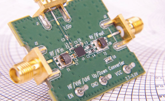
RF circuit boards and Microwave PCBs are used for communication signals in any application that requires receiving and transmitting radio signals. For example, some common applications are cell phones and radar installations.
RF PCB Materials
FR4 materials are acceptable for RF transmission lines and interconnects operating up to WiFi frequencies (~6 GHz). Beyond these frequencies, RF engineers recommend using alternative materials to support RF signal propagation and printed RF circuit designs. Standard FR4 laminates use resin-filled fiberglass weaves to hold components, but these fiber weave effects in certain materials could create signal and power integrity problems if fabrication procedures are not specified properly.
RF PCBs are manufactured with certain materials that fulfill high-frequency operation requirements. These materials should have low signal losses, be stable over high-frequency operation, and should be able to absorb high amounts of heat. The dielectric constant (DK), loss tangent (tan δ), and coefficient of thermal expansion (CTE) values also require consistency over wide frequency ranges. Typical values of dielectric constant range from 3 to 3.5 for these boards. Loss tangent values are in the range of 0.0022 to 0.0095 for the frequency range of 10-30GHz.
Apart from all these specific necessities, the material cost and ease of manufacturing are also considered.
Materials that are made of Polytetrafl uoroethylene (PTFE), ceramics, and hydrocarbons mixed with one another or with a form of glass are commonly used. Rogers material is a common choice for RF circuit boards. There are different variants of Rogers material available.
Alternative material systems use PTFE-based laminates and bondply materials to bond a PTFE layer with the next layer in your PCB stackup. These materials have lower loss tangent than FR4 materials, so signals can travel farther without attenuating and still fall within acceptable margins. These laminates should form the substrate that supports RF transmission lines at very high frequencies, such as 77 GHz radar, or for very long interconnects at lower frequencies, such as 6 GHz WiFi. The table below summarizes some important material properties for common RF PCB materials.
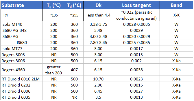
Some dielectric and thermal properties for RF PCB materials
View a comprehensive list of RF circuit board laminates
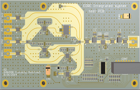
PCB Stackups with RF PCB Materials
Once you’ve selected your laminate and bondply materials for your RF design, it’s time to add them to your stackup. While you could build an entire multilayer PCB stackup with RF materials, it’s generally not needed and can be overly expensive. One option is to build a hybrid stackup, where the RF laminate is placed on a top layer to support RF transmission lines and circuits, and the internal layer is used to support ground planes, routing for digital signals, and power. The opposite layer can also support digital components that need to interface with your RF front end, any ADCs for collecting RF signals, or other components.
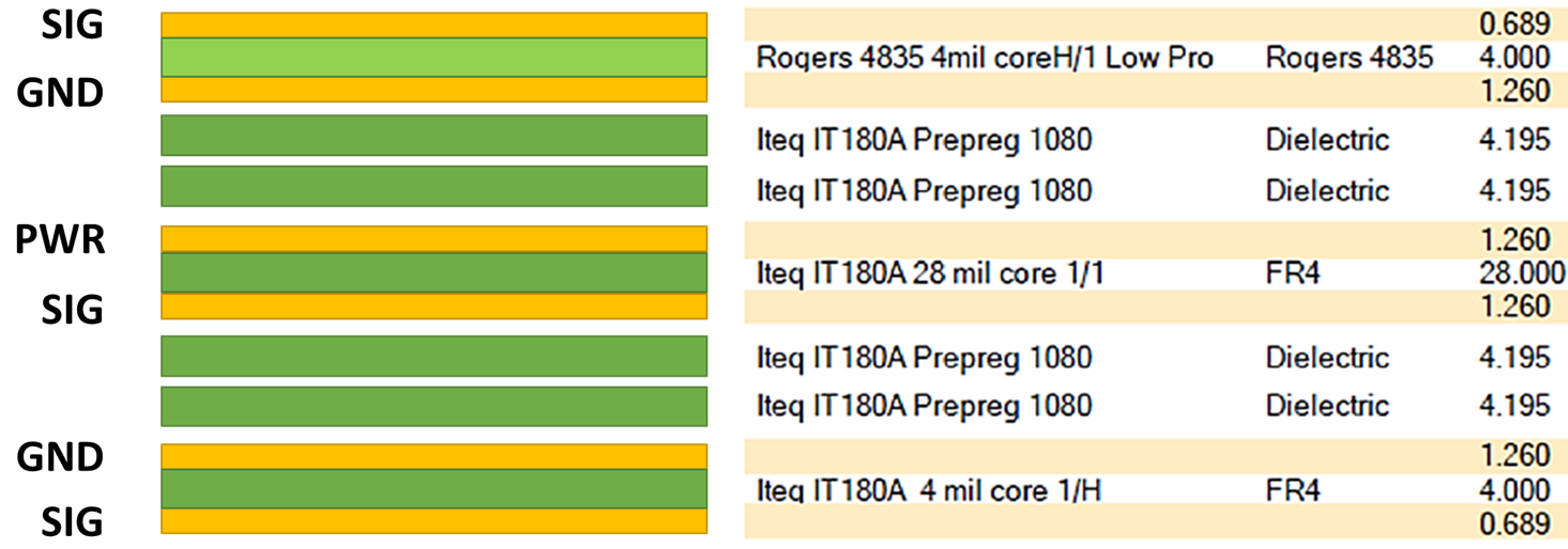
Hybrid stackup with a Rogers PTFE laminate.
If you don’t need a digital section in your RF PCB layout, you can go with a 2-layer or 3-layer PCB with RF laminates that have standard or near-standard thickness. Once you’ve determined the PCB layer thickness and material system, you’ll need to determine the impedance of your RF traces.
Another example without the hybrid material set shown above is given in the stackup table below. In this example, thicker Rogers core materials (RO4350B) are used on the outer layers to provide a thick basis for routing signals on the surface layer with GND on an inner layer. The internal layer is a bondply (RO4450F), and it is used to function as the prepreg that bonds the two cores together. This is just one of many stackup styles used in RF designs. The important point here is the use of bondply layers, which function essentially like prepregs in a standard PCB stackup.
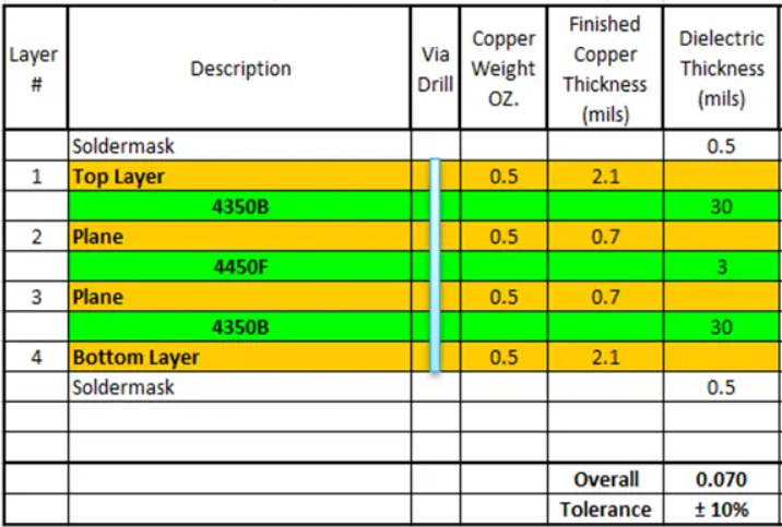
4-layer stackup using only PTFE materials.
Why would we use a stackup with thicker layers to support circuit designs? There are important reasons for doing this that relate to sizing traces to hit impedance targets while also reducing losses, as well as controlling parasitic capacitance/inductance for components in RF printed circuits. The resources below show two examples where thicker outer layers with larger distance to ground are useful for controlling parasitics and thus ensuring impedance matching.
RF PCB Trace Impedance
In a controlled impedance RF circuit, maximum power transfer without distortion occurs from source to load when the impedance remains the same throughout the trace. This impedance is known as the characteristic impedance of the trace(Z0). The characteristic impedance depends on the geometry of the traces, such as trace width, the dielectric constant of the PCB material,trace thickness, and height from the reference ground plane. In order to match these impedances, matching circuits are also designed.
RF trace design
RF traces propagate high-frequency signals and thus are subject to transmission losses and interference issues. The characteristic impedance of these traces is a main concern amongst the designers. In radio-frequency boards, the traces are regarded as transmission lines. The most common types of transmission lines designed are coplanar waveguide (CPWG), microstrip and stripline. Below are the radio frequency trace design aspects that determine proper operation and minimum losses:
- The length of the trace should be as short as possible. This helps to reduce attenuation.
- In the layout, never place an RF trace and a normal trace parallel to each other. If placed like that, interference will occur between the two.
- Ground planes are required to provide return paths for signals.
- The test points are not supposed to be placed on the traces. It will interrupt the impedance matching values of the trace.
- Instead of keeping sharp right turns, gradually curved bends are better for trace performances.
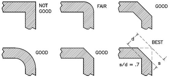 In cases where right-hand bends are unavoidable, a process called metering is used to reduce the ill effects. The metering of a trace is shown below:
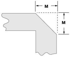 M is given by the following formula:
![]()
Specialized Processing Equipment for RF PCB
Much of the processing for Microwave/RF PCBs can be done on standard fabrication equipment. However, the need for specialized equipment is requires for the most demanding designs. We have invested significantly so that we have in-house: Plasma Etch equipment to ensure that the quality of the thru holes is at the highest level. Plasma etching uses plasmas or etchant gases for the removal of substrate materials in the through holes and to prepare the surface for coating. Laser Direct Imaging (LDI) equipment versus the more traditional photo exposure tools so that we can hold very tight trace widths and front-to-back registration requirements. Laser drilling equipment, which is needed for many of the different materials as mechanical cutting will leave burrs, loosen fabric, or can discolor due to heat. This also allows us to consistently provide microvias to our customers of the highest quality.
RF PCB Capabilities
In addition to standard Microwave/RF PCBs our capabilities using PTFE laminates also include:
- Hybrid or Mixed Dielectric Boards (PTFE/FR-4 combinations)
- Metal Backed and Metal Core PCBs
- Cavity Boards (Mechanical and Laser Drilled)
- Edge Plating
- Constellations
- Large Format PCBs
- Front to back registration of etched cores to +/-.002″
- +/- 0.001″ tolerance on etched features for un-plated 1oz copper
- Blind/Buried, Via-in-Pad, Micro Vias, Stacked Vias, and Laser Via's
- Soft Gold and ENEPIG Plating
- Sequential lamination
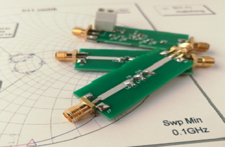
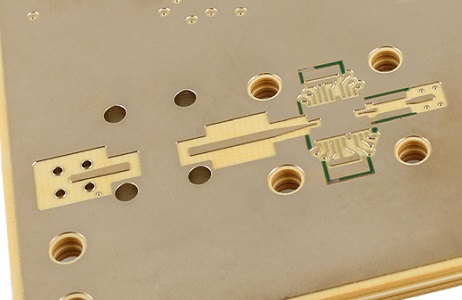
Radio frequency (RF) and microwave (MW) circuits can be found in wireless products from handheld devices for medical and industrial applications to advanced communications systems for base stations, radar and global positioning.
Hemeixin works close with your product design team to insure that the project’s cost/performance targets can be met by providing information on material options, relative costs and DFM considerations.
When producing radio frequency PCBs it is important to think about how to control the signals using (i) materials types and material characteristics (loss tangent / Df and dielectric constant / Dk) (ii) low profile copper foils (iii) weave styles and (iv) how we layout the copper circuitry, as all of these factories have a significant impact on the the performance of the finished product.


