What are HDI PCB boards?
HDI boards, one of the fastest growing technologies in PCBs, are now available at Hemeixin. HDI Boards contain blind and/or buried vias and often contain microvias of .006 or less in diameter. They have a higher circuitry density than traditional circuit boards.
There are 6 different types of HDI PCB boards, through vias from surface to surface, with buried vias and through vias, two or more HDI layer with through vias, passive substrate with no electrical connection, coreless construction using layer pairs and alternate constructions of coreless constructions using layer pairs.
Definition of a High-Density Interconnect (HDI) Printed Circuit Board
IPC-2226 defines HDI as a printed circuit board with a higher wiring density per unit area than conventional printed circuit boards (PCB). There are different types of HDI features, type I, type II and type III as defined in IPC-2226.
IPC-2226 defines HDI as a printed circuit board with a higher wiring density per unit area than conventional printed circuit boards (PCB). They have finer lines and spaces ≤ 100 µm / 0.10mm, smaller vias (<150 µm) and capture pads <400 µm / 0.40mm, and higher connection pad density (>20 pads/cm2) than employed in conventional PCB technology.
Different types of HDI features
The picture below shows the main structures – type I, type II and type III as defined in IPC-2226.
Type I. Defines a single microvia layer on either one or both sides of core. Uses both plated microvia and PTH for interconnection, employing blind, but not buried vias.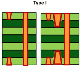
Type II. Defines a single microvia layer on either one or both sides of core. Uses both plated microvia and PTH for interconnection. Employs blind and buried vias.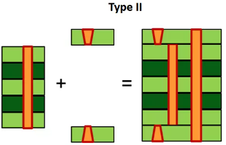
Type III. Defines at least two layers of microvia on either one or both sides of core. Uses both plated microvia and PTH for interconnection. Employs blind and buried vias.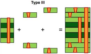
Construction terminology to define the degree of HDI PCB construction:
- 1+n+1 = single layer of microvia (as per the type I and type II examples above)
- 2+n+2 = 2 layers of microvia (as per the type III example above)
- 3+n+3 = 3 layers of microvia
Different kinds of Vias in HDI PCB
Vias are a tiny conductive hole that connects multiple layers in a High Density Interconnect PCB and allows signals to flow through them easily. Depending on the functionality of a PCB, four different types of vias are drilled into a HDI PCB, namely: Through Hole vias, Blind Vias, Buried Vias and Microvias.
- Through-Hole Vias – It is a hole pierced using a drill or laser through the PCB from top to bottom connecting all the layers of the multi-layer PCB. The Through-hole PCB is easy to construct and are the most cost-effective type of vias. The Through holes are further divided into Plated Through (with copper pads) Holes and Non-Plated Through Holes (without copper pads).
- Blind Vias – A type of via where a hole is pierced using a drill or laser to connect the external layer of multi-layer High Density Interconnect PCB to the internal layer. Since the hole is visible only on one side of the PCB board, it is called Blind via. This type of via is difficult to construct and are expensive.
- Buried Vias – A via that connects two internal layers of multi-layer HDI PCB. This via is always inside the printed circuit board and are not visible from the outside. Therefore, it is called buried via. The buried via is also an electroplated hole that needs a separate drill file. The layer count in a buried via is even in number i.e., 2, 4, 6, and on.
- Microvias – It is the smallest vias or holes with a diameter less than 150 microns, drilled using a laser. Microvias are most commonly implemented in HDI PCBs, usually to connect one layer of the PCB to its adjacent layer and have a very small diameter in comparison to the mechanically drilled vias such as through-hole. Due to their size and ability to connect one layer to an adjacent layer, they enable denser printed circuit boards with more complex designs.
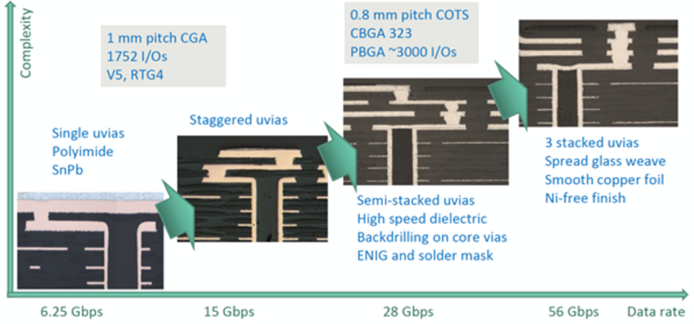
Sequential Buildup HDI PCB Lamination process
The sequential lamination process is predominantly used to build an HDI stackup construction in a layer-by-layer manner. In general, this technique can be used for any multilayer PCB, but it is particularly important for HDI. This is because the high density, very thin dielectrics are formed in individual layers around a thick core, so lamination will happen in multiple steps to build the stackup. The sequential lamination process. This consists of the following steps:
- Photoresist deposition and exposure: This is used to define areas to be etched, which will leave behind a pattern of conductors on the laminate.
- Etching and cleaning: The current industry standard etchant is a ferric chloride solution. After etching, the leftover photoresist can be reclaimed and the resulting conductor pattern is cleaned.
- Via formation and drilling: Vias need to be defined using mechanical or laser drilling. For high via density, the via holes can be removed chemically.
- Via metallization: Once vias are defined, they are metallized to form a continuous conductive interconnect.
- Buildup: Layers are stacked in multiple lamination cycles to build the stackup before outer layer processing.
The standard process used to build the stackup for an HDI PCB is sequential lamination. Effectively, the stackup is fabricated by forming each layer individually, then the entire 2+N+2 stackup is formed with a final lamination step. The most common material types used in sequential lamination for HDI stackups are resin-coated copper (RCC), specifically metalized polyimide, pure polyimide, and cast polyimide. PTFE and FR4 laminates are also used in HDI layer stackups.
Some fabrication houses will tell you that you cannot use stacked vias in a stackup created with sequential lamination, but I think there is some confusion on this point. The 2+N+2 structure can support stacked vias, including with the core via possibly extending into one of the sequentially laminated layers. I think the confusion comes from implementing a stacked via to span two layers as defined in the Type I HDI stackup (see below). Instead, we would use skip vias to route from the surface layer into an inner layer, and this layer pair would be laminated onto the core via layer.
To increase routing density, designers increase the number of layers, producing a complex stack-up. Manufacturers use sequential lamination processes to fabricate such complex designs.
Some of the common types of stack-ups are mentioned below:
- 1+N+1 – PCBs contain 1 build-up of high-density interconnection layers
- i+N+i (i≥2) – PCBs contain 2 or more build-up of high-density interconnection layers. Microvias on different layers can be staggered or stacked
- i+bN+i (i≥2) – Includes buried vias
- Any layer HDI – All the layers of a PCB are high-density interconnection layers. This allows the conductors on any layer of the PCB to be interconnected freely with copper filled stacked microvia structures
HDI PCB vias filling and Capped vias
A via is a copper-plated hole that creates an electric connection between different layers of a PCB. Normally, any type of via such as through-hole, microvia, blind, and buried can be filled. First, the hole wall is plated to make it conductive. Later, the barrel is filled with conductive (copper) or non-conductive (resin) material.
The purpose of filling vias is to:
- Avoid the entry of any impurities. Hence, there is a lower chance of contamination or corrosion
- Improve the mechanical strength of vias and pads
- Place SMT components on the via hole (only if it is resin-filled)
- Strengthen the pad attachment
- Reduce the risk of solder wicking
- Prevent the trimming of silkscreen printing
- Enhance the thermal conductivity and current capacity of a via (if it is conductive filled)
Types of HDI PCB via filling
Conductive filling
Conductive materials like copper or silver epoxy are used to fill the holes. These metals aid in effectively transferring the electric signal and improve the thermal conductivity of the via. The conductive filling can also help to deviate the heat from large components like ICs, BGAs, microcontrollers, and processors.
Copper epoxy has better thermal conductivity, but silver epoxy is more cost-effective.
Compared to non-conductive filling, conductive filling can be expensive. However, it can create a perfect plating of via walls without any voids. This can significantly improve the current flow between the inner layers.
For PCB designs that require to transfer high amount of heat or current from one side of the board to another, conductive via plugging is a handy solution. It can also be used to dissipate excessive heat generated underneath some components. The metallic nature of the fill will naturally wick heat away from the chip to the other side of the board in many ways like a radiator.
Non-conductive via filling or Epoxy Resin Plugging
This does not improve the electrical or thermal conductivity of the via. It provides structural support to the pad in case of a via-in pad. During the PCB manufacturing process, the epoxy paste or resin is filled into regular vias. The walls are still plated with copper for electrical connectivity. It is important to avoid voids in the plating as they can create connectivity issues.
This is the most common and popular method of via plugging, especially for Via In Pad process. The barrel of via hole is filled with non-conductive material. Selection of the material depends on the CTE value, availability, specific design requirements and type of plugging machine. Thermal conductivity of non-conductive material is normally close to 0.25 W/mK. A common misconception about non-conductive via plugging is that the via will either not pass any current or only a weak electrical signal, which is absolutely not correct. The via will still be plated as normal before non-conductive material is plugged inside. It means via will work as normal as in any other standard PCB.
IPC-4761 specifies 7 different types of vias:
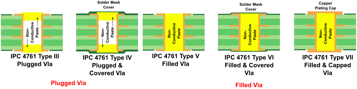
Tended (Via Type I-a/-b) and Tented and covered (Via type II-a/-b) A via with a dry film mask material applied bridging over the via wherein no additional materials are in the hole. Via type II is Via type I with an additional cover. Prior to surface finish. Type II is not supported anymore
Plugged (Via Type III-a/-b) A via or through hole with material applied allowing partial penetration into the via or through hole. The plug material may be applied from either one or both sides of the via structure. (Prior to surface finish.)
Plugging and covered (Via Type IV-a/-b) : A via or through hole with a secondary covering of mask material applied over the plugged via. The material may be applied from either one or both sides of the via structure. (Prior to surface finish.)
Filled (Via Type V) : A via or through hole with material applied into the via or through hole targeting a full penetration and encapsulation of the hole. (Prior to surface finish.)
Filled and covered (Via Type VI) : A via or through hole with a secondary covering of material applied over the filled via or through hole. The material may be applied from either one or both sides of the via structure. (Prior to surface finish.)
Filled and capped (Via Type VII) : A via or through hole with a secondary metallized coating covering the via or through hole. The material may be applied from either one or both sides of the via structure. (Prior to surface finish.)
‘For tented and plugged via types “-a” stands for single sided and “-b” stands for both sides of application.
A type I via is tented during the soldermask process. The downside is that the manufacturer cannot guarantee that the hole is 100% closed. As you can see in the picture on the right, there’s a chance of exposed copper. If you specify this via type, please tent the vias from both sides instead of only one side.
Type III and IV can be specified if you want an inexpensive solution to close the via hole 100%. The via will be plugged from one or both sides.
A Type V or VI vias will be filled with a substance which is normally soldermask or epoxy. IPC does not give a requirement in terms of depth of fill, but Hemeixin does: Boards which are 1.60mm thick, with via holes ranging from 0.25mm to 0.50mm, the target condition is 100% fill, however we consider it acceptable if > 70% fill is achieved.
| Key advantages | Via tenting, type I | Via plugging method: | Via plugging method: | Via plugging method: | Via plugging method: |
| Screen printing, type 3/4 | Normal Through PCB Design, not filled | Non-Conductive Plugging, type VI | Plugging & copper capped, type VII | ||
| Prevents solder from entering the via and over the other side of PCB where it can potentially short components during wave solder process | 100% Not Assured | 100% Assured | 100% Not Assured | 100% Assured | 100% Assured |
| Prevents the solder paste from entering the via and creating a poor solder joint where vias are close to SMD pads – this can affect the dog bone style of the BGA | 100% Not Assured | 100% Assured | 100% Not Assured | 100% Assured | 100% Assured |
What is Ultra HDI PCB?
To be defined as an Ultra HDI PCB, the circuit board must have:
- Conductor width and isolation distance below 50 µm
- Dielectric thickness below 50 µm
- Microvia diameter below 75 µm
- Product characteristics that exceed the existing IPC 2226 level C standard
Ultra-HDI is not a new approach to designing PCBs. The capability, whether subtractive or additive, has been available for very dense PCBs (such as in smartphones) and in IC packaging (in substrates and RDL). The capability was typically only cost effective when volumes were very high, which is why it has enabled some of the highest-compute consumer products and IC production with higher I/O counts. The capability is now becoming more accessible with lower volume fabricators.
The table below lists some of the fabrication features that are typically associated with ultra-HDI.
| Feature | Size limit |
| Linewidth | 20 microns (0.8 mil) |
| Spacing | 20 microns (0.8 mil) |
| Through-hole sizes | 6 mil/12 mil pad (14/16 pad recommended for Class 2/3) |
| Microvia hole | As low as 2 mil laser drill |
| Microvia pad | ~3x hole diameter |
| Via features | Fill & cap (VIPPO) |
| Plating thickness | Up to 0.5 mil hole wall |
| Material thickness for uVia | 2 mil maximum |
| Copper foil thickness | As low as 1/3th oz. |
A couple of the capabilities listed above are typical for standard HDI boards, while others exceed the current standardization defined in IPC-2226 (Level C). For example, in these boards the through-hole via sizing limit is the same as in standard HDI. However, the linewidth limit is much smaller, down to 0.6 mils. Depending on the linewidth, etching may be possible but eventually an additive process would need to be used (e.g., SAP, mSAP, or A-SAP).
HDI PCB Laser Drill Technology
Drilling the smallest of micro-vias allows for more technology on the board's surface. Using a beam of light 20 microns (1 Mil) in diameter, this high influence beam can cut through metal and glass creating the tiny via hole. New products exist such as uniform glass materials that are a low loss laminate and low dielectric constant. These materials have higher heat resistance for lead free assembly and allow for the smaller holes to be used.
Laser Direct Imaging for HDI fabrication process
Imaging finer lines than ever before and using semiconductor Class 100 Clean rooms to process these HDI parts is costly but necessary. Finer lines, spacing and annular ring requires much tighter controls. With use of finer lines, touch up rework or repair becomes an impossible task. Photo tool quality, laminate prep and imaging parameters are necessary for successful process. Using a clean room atmosphere decreases defects. Dry film resist is still the number one process for all technology boards.
Contact imaging is still widely used due to cost of laser direct imaging; however, LDI is a far better option for such fine lines and spacing. Currently most factories still use contact imaging in a SC100 room. As the demand expands, so does the need for laser drilling and laser direct imaging. All of Hemeixin's HDI production facilities use the latest in technology equipment to produce this advanced PCB.
Products such as cameras, laptops, scanners and cell phones will continue to push technology to smaller and lighter requirements for the consumer's daily use. In 1992, the average cell phone weighed 220-250 grams and was strictly for making phone calls; we now call, text, surf the net, play our favorite songs or games and take pictures and videos on one tiny device weighing 151grams. Our changing culture will continue to drive HDI technology and Hemeixin will be here to continue to support our customer needs.
Designing using HDI PCB
HDI is a necessity when the component pitch requires it or the board size demands it. Examples of this include smartphones,wearable technology, and robotics. A properly designed HDI board enables a smaller board (board size goes down), or enables two through-hole (TH) boards being combined into one board (pins per area goes up). A properly designed HDI board has 2X to 3X more average trace lengths per layer than a through-hole board. Some very good HDI designers report 4X performance. So know what your current through-hole design density performance is, and you’ll be able to determine good HDI design performance. HDI boardsare much harder to plan than traditional multilayer boards because, with multilayer, you only have two degrees of freedom, boards size, and signal layers.
HDI has a myriad of constructions and variables that all affect density. To understand how blind vias, skip vias, staggered vias,stacked vias and buried vias contribute to density, you have to do a “routing test” and play with all these different stack-ups and constructions. By measuring the metrics (inches/square inch and pins/square inch), you can create a table that relates these density measures to the corresponding construction.
Use HDI PCB design techniques when considering that need to be mounted on a particular size of board—or the average connections per square inch of board is extremely high. If the connections of all the parts and test points divided by the size of the board is less than 120 — 130 pins per square inch, there is no need to be using HDI.
PCBs have revolutionized the electronics industry and are used in every electronic gadget you know. The demand for Printed CircuitBoard (PCB) looks promising as it is extensively used in various industries as mentioned earlier. The HDI PCBs have gained momentum in recent years due to their versatility. The 10 layer HDI are major drivers in the HDI PCB market. With HDI design,designers can create smaller products with improved signal integrity and make electronics fit anywhere they are needed.