What are Rigid Flex PCB?
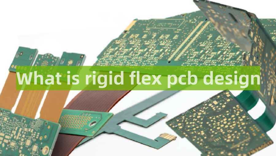
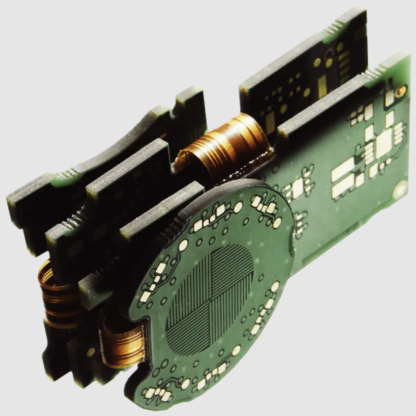
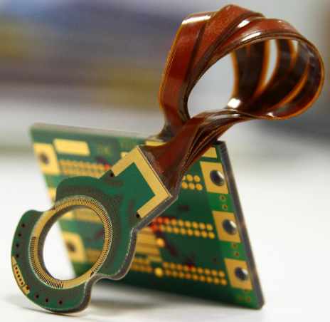
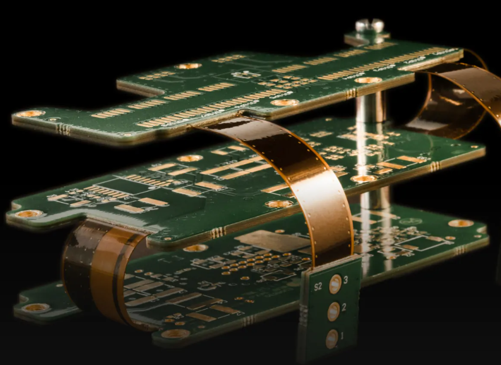
Rigid flex printed circuit boards (PCBs) provide designers with one of the more unique packaging methods for electronic designs. Combining the component and routing density of hardboards with the flexibility of flexible circuits, rigid flex PCBs allow designers to achieve routing density and interconnectivity that is not available in other types of circuit boards.
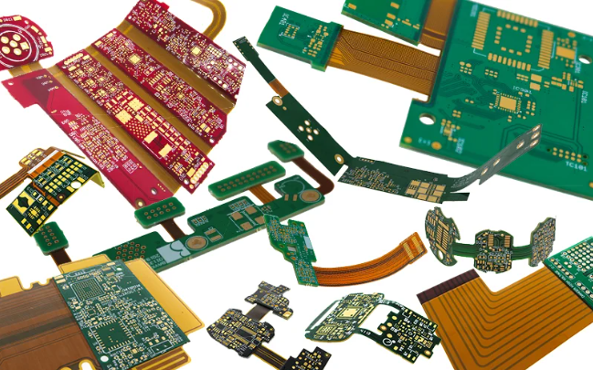
Rigid flex circuits have been used in the military and aerospace industries for more than 40 years. In rigid flex circuit boards, layers of flexible and rigid materials are used to create both rigid and flexible areas in a single package.
Rigid flex circuits combine the best of both rigid boards and flexible circuits integrated together into one circuit.
Rigid outer layers are connected to inner flexible layers using copper plated vias. Rigid flex circuits provide higher component density and better quality control. Designs are rigid where extra support for SMT components is needed, and is and flexible in areas that need to bend and flex to fit into tight spaces.
Rigid flex PCB benefits
There are many high level benefits to Rigid Flex PCB including:
- Connection Reliability – Connecting rigid layers with flexible cables is the foundation for combination rigid flex circuits.
- Lower Part Count – Compared to a traditional rigid board, combination rigid flex circuits require fewer parts and interconnections.
- Flexible Design Options – At Hemeixin, we pride ourselves on taking on the most complex of design challenges. Rigid flex circuits can be designed to meet highly complex and unimaginable configurations while utilizing a rigid substrate.
Rigid flex circuit designs could entail any of the following:
- Highly complex configurations
- Controlled Impedance
- Three to eight-layer combinations
- Reduced interconnections
High Density Applications – More often than not, the rigid component of a rigid flex circuit is utilized for high density device population. In addition, flexible circuits allow for minutely narrow lines giving way to high density device population. Denser device populations and lighter conductors can be designed into a product, freeing space for additional product features.
Package Size and Weight Reduction – Multiple systems in rigid boards create more weight and utilize more space. Combining rigid boards with flexible circuits allows for a more streamlined design thus reducing package size and weight.
Rigid flex PCB advanced features
As the Rigid flex circuit market continues to expand, there have been many advances in technology including:
- Air Gap – Through the process of selective bonding, increased flexibility is achieved by “unbonding” layers so they are allowed to flex freely. At Hemeixin, we are fully capable to support air gap technology applications allowing your designs more flexibility.
- Component Assembly – Hemeixin offers through hole and surface mount capabilities, as well as in circuit testing, conformal coating and electrostatic protective packaging.
- Controlled Impedance – With increasing signal switching speeds, engineers need to understand and control the impedance of sensitive signal lines. With short signal transition times and high clock rates of modern digital circuitry, traces need to be considered transmission lines rather than simple interconnections. With today’s higher speed requirements, controlled impedance traces are designed to minimize electrical reflections and ensure an error free transition between the trace and terminations. Controlled impedance requires tight control of the physical dimensions of the etched copper traces (width and thickness), and also the thickness of the dielectric materials. Controlled impedance signal transmission requires flexible circuit materials to be uniform in both thickness and electrical properties.
- Panelization – Multiple circuits are partially routed with break-away tabs to allow them to remain in the panel for component assembly during the “pick & place” and wave soldering processes. Once the panel of rigid flex circuit boards are assembled, simply clip them out by cutting or v-scoring the break-away tabs and they are ready for assembly into your final product.
- Shielding – Shielding is typically specified when an application requires controlled impedance, and/or limits in electromagnetic and/or electrostatic interference. Common shielding options are:
Copper (solid or cross hatched)
Shielding film (e.g. Tatsuta)
Silver or carbon ink
Rigid flex PCB applications
There are two main functional applications for rigid flex. These are static (flex-to-install) and dynamic (continuous flexing over the life of the product). The design and construction of the rigid flex will be dependent on whether the application is static or dynamic.
Static Application – An application where the flex circuit is only required to flex during installation in order to fit it into its application (also known as flex-to-install).
Dynamic Flexing Applications – An application where the flexible area is dynamically flexed during normal operation. This can range from a few hundred cycles up to over 1 million cycles.
Advances in rigid circuit board technology has broadened the applications in electronic products from computer, communication, and consumer electronics, to automotive, medical, and military electronics. Increasing demand for more powerful and smaller products drives the need for multiple layers to accommodate denser, finer line width and spacing and smaller hole sizes.
When Should You Use Rigid Flex PCB?
- When a designer needs a flexible solution & needs to rout components on both sides of the PCB
- When a designer requires electronics fit the device, rather than the device conform to the electronics
- When the electronic components & connectivity required max out space for connectors & flex cables
- As a single-package solution for electronics with high input/output connectivity
- As a cost-effective alternative to a combined assembly of interconnected hard boards
- When the designer has to miniaturize their design to accommodate greater functionality
- In weight-saving applications, such as drones, unmanned vehicles, aerospace & space applications
- High vibration environments
- High shock applications – where electronics will be subjected to 10,000+0 G-s
- In never-fail electronics
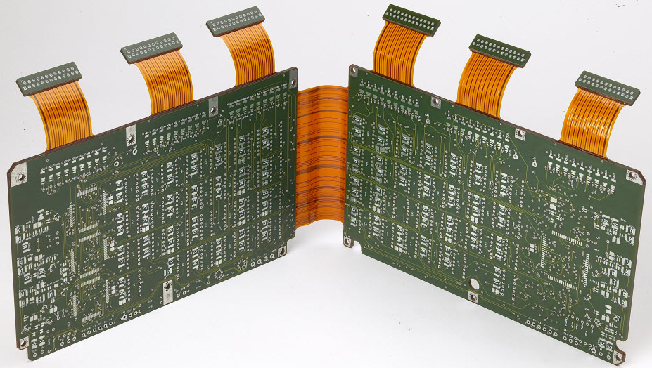
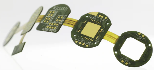
Rigid-flex circuit boards offer the best of both worlds when used for portable devices. The flexible circuit area works well for products that require it to bend in certain places, while the rigid circuit area provides stability and strength to other areas of the product that require enhanced durability and shock absorbance. Some of the main advantages consist of the following aspects
Reduced Packaging
By combining rigid circuit boards and flex circuits into one integrated unit, the need for wired connections becomes significantly reduced and, in some cases, eliminated. The flex area materials take up 10% of the size and weight compared to wired solutions, allowing the customer to come up with product designs that are lighter and smaller in size when required. One rigid-flex circuit board can fit in places where multiple rigid boards, connectors, and wiring harnesses would not be able to, and its tighter bend capabilities offers interconnect solutions not available with any other solution.
Higher Reliability
One of the issues with using multiple rigid circuit boards is that many more interconnects are required. Contact crimps, solder joints, and connectors not only take up space but also create potential points of failure if the product is accidentally dropped during use. In some industries, such as medical and military applications, anything less than the highest possible level of reliability could lead to dangerous or disastrous circumstances.
Rigid-flex circuits offer higher reliability to shocks and vibrations. They maintain their high performance during drop testing due to the reduced points of interconnect. The product also becomes more lightweight which reduces the likelihood of potential failures.
Higher Capabilities
The flexible PCB areas in rigid-flex circuit boards offer a higher range of capabilities than traditional rigid circuit boards with wired interconnects. When the product design requires high-speed signals and controlled impedance, the flexible board can handle the transmission loads effortlessly. The flexible areas can also provide high levels of shielding for EMI and RF interference from either component within the product or from outside sources. Another benefit to rigid-flex circuits is that they work reliably even when being used for applications in harsh environments. The boards have good corrosion resistance, chemical resistance, and UV resistance. They can also handle higher temperatures up to 200°C while being able to dissipate generated heat.
Potential Cost Savings
When customers select a rigid-flex circuit board for their application, they may find potential cost savings due to lower material use and easier assembly. The rigid-flex circuit can be designed into smaller and lighter packaging, as customers will only need to pay for the reduced amount of materials that will be used for the final assembly. These cost savings may also be reflected in the fewer components and connectors required.
Rigid-flex circuits can accept any type of component or connector that a regular rigid circuit uses. The product design will not need any special connectors or components to combine the rigid and flexible PCBs together or to other components. Rigid-flex circuit boards are also easy to assemble and install. There is only one way that they can be installed, as this reduces assembly errors that would require an entire new rework.
Rigid Flex PCB Technology and Production Process
Whether producing a rigid flex prototype or production quantities requiring large scale PCB fabrication and PCB assembly, the technology is well proven and reliable. The flex PCB portion is particularly good in overcoming space and weight issues with spatial degrees of freedom.
Careful consideration of flex-rigid solutions and a proper assessment of the available options at the early stages in the PCB design phase will return significant benefits. It is critical the PCB fabricator is involved early in the design process to ensure the design and fab portions are both in coordination and to account for final product variations.
The manufacturing phase is also more complex and time consuming than rigid board fabrication. All the flexible components of the rigid flex assembly have completely different handling, etching and soldering processes than rigid FR4 boards.
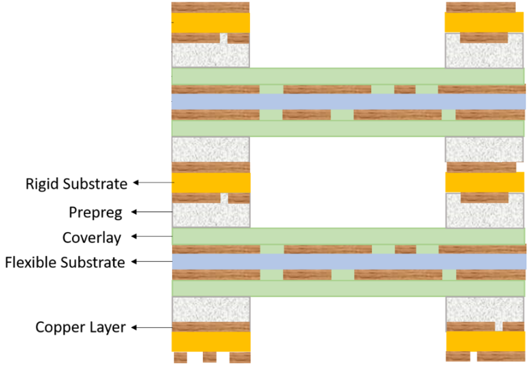
Rigid-flex PCB Stackup
Once you move on to rigid flex PCB design, you’ll need to define your flex ribbon using a similar stackup as your rigid PCB. Flex ribbons are thinner than the boards with which they interface, and the flex ribbon will need to have the same stackup as the inner layers in the rigid printed circuit board. Flex ribbons typically need to carry signal between boards, and they will also need to have a ground return connection.
If you intend to extend a power or ground plane all the way across the flex ribbon, use a cross-hatched copper pattern. Cross-hatched copper provides improved flexibility over a solid copper film or copper foil. Cross-hatched copper should also be used if you need shielding for signal layers on the flex ribbon.
Flex ribbons do not need to have the signal layer placed directly below the coverlayer on the flex ribbon unless you plan to place components directly on the ribbon. You can place SMT components placed directly on the ribbon as long as there is a signal layer below the coverlay. This is becoming a more popular design choice.
Solder lands need to be placed in the signal layer directly below the coverlay, and the coverlay needs to have holes punched so that SMT components can access the signal layer. Always check with your fabricator and make sure that their capabilities will accommodate your design choice. Always avoid placing these features and components directly in the bend area, and place components so that the length of the component is parallel with the bend.
An alternative method for placing components on a ribbon involves button plating. The signal layer still needs to be placed below the coverlay in the stackup, and punched holes in the coverlay are also used to access the signal layer. A through hole via is placed in the mounting pad, and the structure is then plated up to a specific thickness. If the via holes are left open, through hole components can then be placed on the flex ribbon.
Your PCB board design software should allow you to define rigid flex stackup without requiring extra design steps or specialized tools.
Rigid-Flex PCB Layer Stackup
There are many different layer stacks that can be used in a flexible PCB or in a rigid-flex PCB. The most basic uses a single flex region with two copper layers built on a flexible substrate material (polyimide) as shown below. This flex region can be directly incorporated into a rigid-flex PCB stackup or it can be used on its own. In a rigid-flex PCB, the coverlay film is bonded to the prepreg during lamination so that the FR4 stiffener regions can be assembled on the flex ribbon.
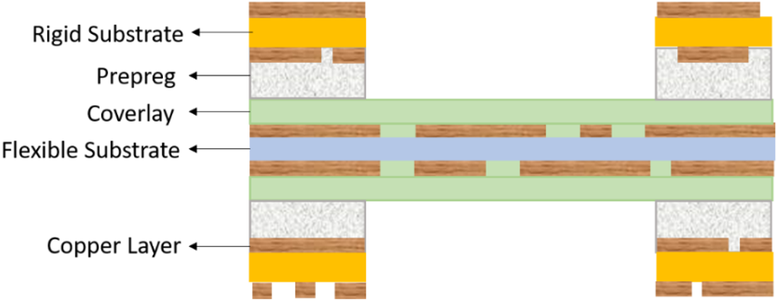
The rigid-flex stack-up typically consists of at least one flexible layer pair between rigid sections. The most commonly designed rigid-flex boards usually have double-sided flexible PCB laminated with rigid sections with layers of pre-preg as shown in the above figure.
Note that the stiffener sections use a prepreg to bond to the flex section in each of these arrangements. However, the layer stack shown above does not need to be limited to a single internal copper layer and two rigid FR4 layers. Multiple rigid layers can be stacked on each side of the flex region. Also the FR4 layers on each end can have different layer counts as these will be laid up and press laminated individually.
Multilayer Flex PCB Stackup in rigid flex pcb
Two flexible layer pairs are usually not stacked on top of each other when the flex ribbon is just being used as an integrated connector. However, if we are talking about a multilayer flexible design, then multiple coverlay-substrate layers can be laminated in succession to give a multilayer flex PCB.
The above image shows four flex layers, but realistically we can have an odd number of flex layers by bonding substrates directly and etching away one layer. Flex fabrication houses can help with planning a flex PCB stackup with an odd layer count.
Bookbinder Rigid-Flex PCB Stackup
We can also have multiple rigid layers between stacked flex regions in a bookbinder-type flex stackup. In this stackup, the flexible layer pairs are stacked on top of each other with some prepreg creating space in between the flex ribbons. By making one of the flex regions slightly longer, the entire stack can be folded without creating excess stress on the outer flex ribbon layer. This is outlined below.
Due to the diverse range of options in building flex PCB layer stackups, designers should contact their fabrication house to make sure the stackup they want can be reliably fabricated. Flex and rigid-flex PCBs offer many unique design approaches, but designers should check to ensure their idealized stackup can be produced as intended.
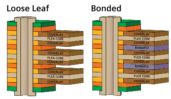
Coverlays and bondpiles
Coverlays are flexible materials, typically on the outside of a flex substack, that protect and insulate the flex circuitry on surfaces and prevent it from lifting. A typical coverlay construction has a polymide dielectric on top and an adhesive on the side facing the copper. Bondpiles are similar to coverlays, but they are used on inner stripline layers, with adhesive on both sides and the polymide dielectric in the middle. They are used to glue two flex cores together.
Rigid flex PCB Surface finishes:
- ENIG (Electroless Nickel Immersion Gold)
- ENEPIG (Electroless Nickel Electroless Palladium Immersion Gold)
- Solder (Tin/Lead RoHS compliant)
- Hard nickel/gold
- Wire bondable gold
- Tin
- Organic Solderability Preservative (OSP)
- Silver
Rigid flex PCB materials:
- Polyimide (Kapton) 0.5 mil to 5 mils (.012mm – .127mm)
- Adhesiveless copper clad base material 1 mil to 5 mils
- Flame retardant laminate, base material, and Coverlay
- High performance epoxy laminate and prepreg
- High performance polyimide laminate and prepreg
- UL and RoHS compliant material on request
- High Tg FR4 (170+ Tg), polyimide (260+ Tg)
Rigid-flex PCB design Tips
Bending and folding
The key reason for making a flex design is so that it can be bent or folded. Rigid flex PCB design tool includes a draw object, called a “bend area,” the location of which defines where the bend happens.
Route along curving boards
When you have a curving flex cable and as many signals that can fit with a tight squeeze, you need a special routing algorithm that can follow the contour of the board outline and automatically insert all the signals required. In Rigid flex PCB design tool, all curved traces use true arc primitives.
Design Rule Checking (DRC)
Rigid flex PCB design tool is unique in its ability to generate and maintain these dynamically and have a DRC that reports if a tear drop fails.
When considering between rigid circuit boards or flexible circuit boards for your application, gain the best of both worlds with rigid-flex circuit designs. They provide strength, high-speed capabilities, reliability, and potential cost savings to your application. These circuit boards also broaden the possible design specifications when the product may require to be built in smaller and lightweight sizes that alternative interconnect solutions may not be capable of. Relying on the best of both rigid and flex circuit capabilities in one integrated rigid-flex PCB design permits the customer to obtain the packaging and performance required for many of today’s high-performance portable devices.


