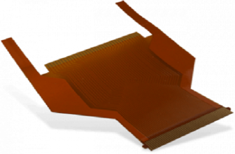
What is High Density Interconnect Flexible Circuits
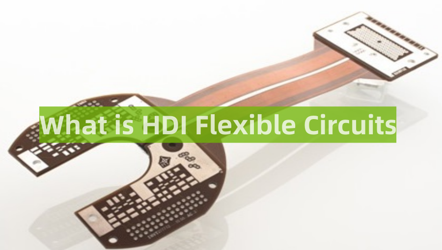
Running out of real estate with conventional feature sizes? Hemeixin High Density Interconnect flex circuits can improve electrical performance and consistency by using vias as small as 50 microns or 9-micron copper to increase density in a small electronic package.
Hemeixin is one of the first companies to provide volume HDI capability to our global customers. Our continuous investment in developing processes for world-class fine-line µVia technology helps us maintain our position as a leader in sophisticated HDI manufacturer. We provide complete solutions to our customers by early design reviews to help eliminate potential cost or yield challenges, shortening NPI and production cycle times, and delivering reliable, high-quality products in the most cost-effective ways.
Today, Hemeixin boasts the capabilities for up to 18+ layers of vertically-stacked and copper-filled µVias. Combined with additional innovations in 0.3mm fine-pitch package support, edge plating, and active cavity structures, Hemeixin offers our customers the flexibility to meet any design challenges. These integrated processes are critical to the thin, high-density assemblies required in the smartphone, computing, IoT devices, modules, and many other products.
Hemeixin is ready to provide you with end-to-end engineering and production services to bring your next-generation product PCB requirement seamlessly from NPI to mass production with world-class cycle times.
We are working with polyimide foils as thin as 12.5 µm and adhesive bond plies starting at a thickness of 12.5 µm. State of the art equipment enables us to produce FPCs with high output, reliability and repeatability. Depending on the dielectric thickness, laser drilled blind via’s can be as small as 35 µm in diameter and filled with copper in the subsequent plating process to support the use of stacked via’s and via-in-pad structures.
High-end alignment tools make it possible to achieve very small annular rings and solder mask registration even on extremely complicated multilayer FPCs. As an option, also cover layer foils can be used.
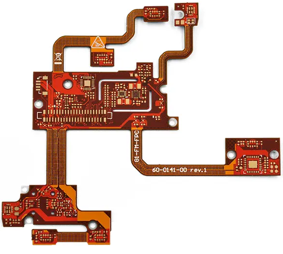
High accuracy laser contour cutting & optimized the space utilization make it possible to achieve excellent 3D miniaturization for small wearable (medical) devices as well as high signal density COF (chip on flex).
Benefits of High Density Interconnect Flexible Circuits
High Density Interconnect flex circuits offer designers the same benefits of flex circuits—smaller, more reliable products—except at a higher level. In addition to the design benefits of HDIs and micro-via’s listed below, HDI circuits give you more design, layout and construction options helping you finish your design in less time.
- Lower cost and smaller size – increased circuit density can eliminate extra layers and save up to 40% compared to non-HDI designs.
- Use advanced component packaging – high-I/O and fine-pitch feature capabilities possible with HDI.
- More design options and flexibility – blind and buried micro-via’s allow for conductor routing on the internal layers under via’s, creating more usable design space per layer.
- Improved electrical performance and signal integrity – micro-via’s in high-speed circuits improve electrical performance by allowing shorter circuit paths, stub reduction and lower cross talk and noise.
- Improved thermal performance and reliability – micro-via’s lower the z-axis thermal stresses between adjacent layers.
- Improved cost effectiveness – Intelligent panel size maximizes circuit density to increase the efficiency of your assembly process.
High Density Interconnect Flexible Circuits Features
- 3-20 layer HDI flexible PCBs
- Circuit board structures down to 25μm
- Laser micro via’s down to 35μm diameter
- Annular rings down down to 50μm diameter
- Minimum copper thickness: 9 micron
- Minimum microvia size: 75 micron, 50 micron finished
- Copper filled blind via’s
- Stacked & staggered micro via’s
- Thin base materials down to 12.5μm
- Complex contours and depth milling
- Laser cavities
- Edge plating
- Panel and reel-to-reel production
- Extensive portfolio of surface finishes for all assembly methods
HDI Flexible Circuits Applications
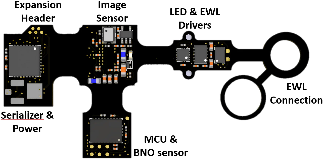
Wearable technology is one of the new applications we are seeing where dense packaging is required. Imagine wearing a sensor device that can monitor all of your vitals and connect to the internet via Bluetooth so your doctor can monitor you remotely. The solution has to be bendable, stretchable, and dense. We will talk more about this in upcoming columns, but this is the type of application that drives density.
Equipment for HDI Flexible Circuits
Gone are the days of plants with rooms full of noisy drilling equipment. HDI requires smaller holes and blind and buried vias that are best done with laser technology. Lasers provide a faster, more cost effective solution over drilling (after you get over the sticker shock cost of the equipment).
HDI Flexible Circuits Materials
Very thin copper materials are essential to creating high density solutions. Nine-micron copper is what is used in many cases to create HDI solutions. Thinner materials are on the horizon. New higher speed materials—coverlays and adhesives—are being qualified on a daily basis to meet the challenges of higher speeds and impedance requirements.
HDI Flexible Circuits Lines, Spaces and Hole Sizes
Smaller lines and spaces are required for HDI. Today, 50-micron (2-mil) lines and spaces in production and 37.5 microns (1.75 mils) line and spaces are being provided in prototypes. The laser drill enables smaller hole diameter (50-micron hole diameters) and enables blind and buried vias for even denser packaging.
HDI Flexible Circuits Assembly
Many industry flex circuit gurus discuss HDI with regard to the density of the package—the circuit itself. However, in addition to the package, an HDI flex requires HDI assembly—the need to place 1005 components and 12-mil pitch BGAs.
High density interconnect flexible circuits manufacturing
Flexible printed circuit boards (FPC) are offering the highest level of 3D miniaturization. Very low bending radii in combination with ultra-HDI (ultra-high density interconnect) are enabling our customers to build increasingly smaller and highly integrated devices. This technology is an enabler of small wearable devices as well it provides high signal density.
Hemeixin has been a market leader in this field for many years and is manufacturing flex circuits with a layer-count of 1 to 8. We are working with polyimide foils as thin as 12.5 µm (0.5 mil) and adhesive bond plys starting at a thickness of 12.5 µm (0.5 mil). Our state of the art equipment is enabling us to produce FPCs with high output, reliability and repeatability. Depending on the dielectric thickness, laser drilled blind vias can be as small as 30 µm (1.4 mil) in diameter, and can be filled with copper in the subsequent plating process. This plating technology is enabling the use of stacked vias and via-in-pad structures.
Leading edge alignment methods are enabling us to achieve very small annular rings and soldermask registration even on extremely complicated multilayer FPC. As an option, also coverlayer foils can be used.
All standard surface finishings can be deposited on the boards, providing our PCBs with finishings for all assembly methods used.
High accuracy laser contour cutting is generating radii of 0 µm and is optimizing the space utilization and enabling our customers to achieve excellent 3D miniaturization.
Flex Printed Circuits (FPC) have numerous advantages over their rigid circuit counterparts. In the pursuit of continuous miniaturization, FPC material properties enable smaller application form factors with the benefit of reduced weight and optimized volume utilization. In addition to facilitating designs with ultra-dense and precise conductor geometries, polyimide based flex materials provide excellent electrical performance characteristics. All of these attributes are indispensable to an electronics industry that is driven to the everchallenging quest to extend functionality on continuously smaller footprints.
With innovations like Hemeixinstrate and the plasma-etched microvia, Hemeixin is an enduring pioneer of flexible multilayer HDI and Ultra-HDI boards. We are empowered by an unquestionable commitment to serve this business segment. As a technological frontrunner, Hemeixin is equipped to cope with cutting-edge design requirements and the most demanding quality standards as applied in the medical and defense industries.
Our high yield manufacturing of HDI and Ultra-HDI flex applications and professional, hands-on consulting services are compelling reasons to make Hemeixin your FPC partner of choice.


