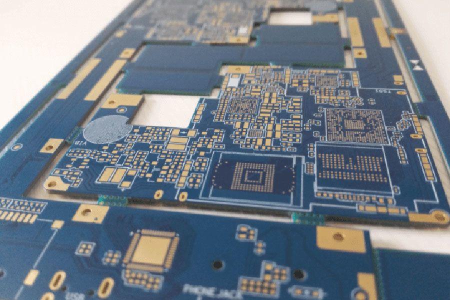
What Affects HDI PCB Cost?
Our production is fine-tuned to manufacture high technology HDI PCB. Products include large and thick HDI PCB and also very high density thin stacked microvia constructions.
HDI PCB and Advanced HDI PCB technology enable design for very high-density components like 400u pitch BGA with a high amount of I/O pins. This component type usually requires an HDI PCB using multiple layer HDI, for example, 4+4b+4. Hemeixinpcb’s HDI PCB manufacturing is specialized in express production of this HDI PCB type.
If small (16 mil diameter/8 mil hole size or smaller) via sizes are required, HDI PCB is often the only answer.
HDI PCB generally raises the cost of a PCB by 2x, unless the PCB is:
- Very small (like a cell phone)
- Extremely complex and dense (many large pin count devices like an aircraft A/V distribution system board)
HDI PCB -High-Density Interconnect printed circuit board
- Laser drilled blind vias (<13 mils diameter) on 1 or more layers, often with a thru-hole board sandwiched in between.
- Can have stacked vias (laser or mechanical)
- Adds significant cost because of the additional steps (time) required and equipment cost.
What Affects HDI PCB Cost?
For this reason, via hole size (which dictates diameter) and HDI PCB layer count have the most major HDI PCB price impact.
- 1. Via size; makes HDI PCB /nonHDI PCB decision
- 2. Layer count; adds to cost of materials + yield loss
- 3.Trace/clearance size; impacts yield loss
- 4. Special vias (blind/buried/etc.) impact time and yield,adds cost. and yield, so adds cost.


