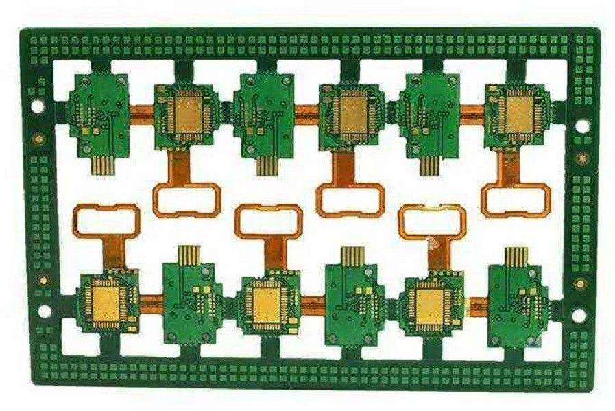
Flex pcb fabrication process
Flex PCB is one of the most important technological advances made in the field of electronics. Despite the complexity and cost-burden associated with the flex circuits, they are widely used. Especially in the still-evolving wearable electronics and devices where package design is more important than maintaining a reasonable cost.
It’s important to understand the manufacturing process of a flex PCB. Understanding the steps and processes a circuit goes through when it’s with the fabricator or manufacturer, can offer designers a wider perspective. If they can comprehend the process from the assembly and manufacturing line perspective, they can adopt practices that may allow them to save on the cost, and increase the durability and functionality of the circuit. That’s especially important for flex circuits where mechanical construction of the circuit is just as important as its electrical characteristics. And manufacturing steps have a significant impact on the mechanical side of the circuit.
Flex PCB Manufacturing Process
When you are designing a flex PCB, make sure you have considered every important detail. The bend radius, neutral bend axis, component placement, plated through-hole placement, SMT components, trace width transition and continuity, and copper layer thickness. Any of these, and a number of other things, can result in a flex that either doesn't function they you intended it to or isn't very durable. Once the design is ready, confers to the design guidelines of your fabricator, and sent to them in the recommended format, the manufacturing process begins. The time to manufacture a flex PCB depends upon the complexity of the design and the capabilities of the fabricator.
- The first step is preparing the core material. The most commonly used material is the PI substrate. The copper is deposited on the flex layer using the annealing method. Electrodeposited copper, even though it offers superior conductivity, cannot be used on flex because it doesn't offer the same mechanical flexibility that Annealed copper does. Your manufacturer doesn’t necessarily have to have facilities for this process; they may simply buy high-grade PI substrate with the annealed copper layer.
- The next part is cleaning the sheets. The manufacturer has to be certain that the flex core/substrate is perfectly clean and clear of any dust particles. These particles can create shorts or breaks in the flex circuit in later stages of the process. These sheets are either cut before or after the cleaning process to accommodate the panel sizes for further processing.
- The next step is drilling. For mechanically drilled holes, a CNC machine is used. It’s usually part of the full fabrication line of the flex PCB manufacturing. The microvias are drilled at that stage too. For multilayer circuits, the microvias can be buried, or a continuation of staggered or stacked microvias. Plated through-holes aren't usually needed on the single-sided flex. For double-sided flex, plated through holes are drilled at that stage too. Drilling and plating both are done at this stage of the process. Other holes may include alignment holes, testing vias, and other component holes.
- When the copper-clad substrate sheets are ready, the manufacturers proceed to the next process of transferring the pattern. The cleaned sheets are first coated with a photo-resist/etching-resist film on one or both sides. The sheet is photosensitive and can take in the pattern of a dry photo film with the circuit pattern on. The photo-resist film is layered over the copper surface by passing it through a hot roller, that laminates the film on it. Once that’s done, the substrate is sandwiched between the photo-layers with the circuit pattern. The alignment holes make sure that the films are placed exactly in the right place. If there is any discrepancy between the top and bottom layer pattern of the flex PCB, the circuit simply won’t work.
- The actual pattern transfer happens thanks to strong UV lamps. These lamps transfer the film pattern over the photo-resist film that’s coating the copper, protecting the copper beneath the pattern. Once the circuit is exposed and the pattern properly transferred, the non-exposure areas can be removed to reveal the copper underneath. The copper can be removed through the etching process, leaving the patterns intact. It’s important to understand that that UV lamp exposure and etching are fairly common processes, and many people have developed DIY devices for these purposes to made home-made circuits. And while this may work with common and simple rigid boards, doing so on a flex circuit is completely different. A flex circuit is handled by professionals in a very controlled environment to make sure it’s not exposed to unsuspected UV lights between exposure and etching to create any unwanted connection. So make sure you are getting your flex manufactured/fabricated by professionals who have the right facility, tools, and expertise.
- After the etching is done and unwanted copper removed, the film covering the copper patterns and traces is “stripped” away. The process may be a bit different and lengthy for double-layered flex circuits. Some fabricators have facilities in place for an AOI, automated optical inspection of the circuit to make sure nothing is amiss before they proceed further.
- After that, the surface finish is applied to protect the circuit. Just like solder-masking is done for the rigid-circuits, a coverlay is laid over the flex circuits to keep it protected. It's an insulating layer, and the material is usually PI, the same material used mostly as the flex substrate. The circuit is then run through a hot press to laminate the coverlay on the circuit properly. Some fabricators run another surface finish on the circuit at this stage. And after that, the bonding is usually coated with gold or nickel to protect the terminator function.
- Silk screening is needed if there is any information, designer, or fabricator’s copyrighted marking needs to be visible on the circuit. When that's done, the circuit is usually electrically tested by the quality control department, and after that, it's ready for component placement or shipping.
Conclusion
The steps mentioned above are usually followed by most of the fabricators, with some exceptions. Still, one fabricator can be wildly different from another. They can have a different level of expertise, different fabrication capabilities, and instruments. As a designer, you want your circuit to translate seamlessly from conception to fabrication, and for that, you need to work with professionals who employ cutting edge technology, and have a lot of experience designing different types of flex circuits. Fabricators like these could analyze your design and perceive problems even before the flex pcb is passed through the first step of manufacturing.


