Types of HDI PCB
A High-Density Interconnector Printed Circuit Board, or HDI PCB, refers to a circuit board with a greater wiring density per unit of area than a standard board. HDI PCBs have narrower lines and margins, fewer vias and capture pads, and a greater density of connecting pads.
It aids in the improvement of electrical efficiency as well as the reduction of device size and weight. For high-layer-count and expensive laminated boards, HDI PCB is the superior choice.
HDI PCB has numerous advantages, including high speed, compact size, and higher frequencies. It is the most important component of laptops, desktop computers, and cellular phones. HDI PCB is now widely used in different end-user goods such as MP3 players and gaming consoles, among others.
Inter-surface through vias, with buried vias, and through vias, a passive substrate with no electrical connection, coreless construction using layer pairs, two or more HDI layers with through vias, and alternate coreless constructions utilizing layer pairs are the six different forms of HDI PCBs.
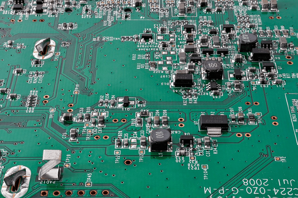
Manufacturing HDI PCBs
HDI PCBs necessitate a high level of technical specialization, meticulous methods, and specialized equipment. Plugging, laser imaging, laser drilling, and sequential lamination cycles are all employed in the process of manufacturing HDI PCBs.
Although standard PCBs are usually made with the use of acid, laser drilling technology is important for HDI PCBs. As this technique is expensive, some contact imaging processes are still employed today. Lasers, on the other hand, are the greatest alternative for the design process because the pathways to other elements must be narrow and compacted.
As a result, several of the common problems that technicians have with PCBs, such as sharp angles, would not be a concern with HDI PCBs.
Precautions need to be taken while manufacturing since the pathways are finer, there are more components present, and this means that there are more electrical signals being transmitted. High-frequency transmission capabilities, impedance management, and a method to eliminate unneeded radiation must all be included in the engineer's plan.
Multilayered designs with insulating materials are employed to achieve this. This creates multiple pathways on narrower HDI PCBs, which are then laminated to let the product that the HDI PCB will operate function completely.
The HDI PCBs are assembled using a lamination process once they've been etched. The layers are stacked on atop one another using a hot roller. The elements are preheated to ensure that all boards have a stable and constant exit temperature.
Types of HDI PCB
Fabricators can employ HDI PCB stack-ups of types I, II, III, IV, V, or VI, according to the IPC-2315 standard from the Institute of Printed Circuits (IPC). Types IV, V, as well as VI are somewhat pricier to manufacture and are typically not suited for HDI PCBs with routing or BGA breakout difficulties. Hence, we will only discuss the three most common ones.
Type I
A laminated core with at least one layer of microvias on one or either side characterizes Type I stack-up HDI PCBs. PTH and blind vias are allowed in Type I HDI, but buried vias are not.
In order to sustain reasonable reliability, the total length to hole diameter or the aspect ratio for the plated through-hole should be above 10. One thing to keep in mind is that under the extreme temperatures necessary for lead-free soldering, very thin FR-4 dielectrics can delaminate.
For larger dense circuit boards with multiple pin-count BGAs, the Type I HDI stack-up is not necessarily better than the laminate since the PTH via pads will have to get larger for greater layer counts. Furthermore, with the development of unique features like smaller diameter vias or finer traces, the usage of a single microvia layer does not provide substantial advantages.
Type II
Microvias, buried and blind vias, and at least one layer of microvias on either or both sides are used in the construction of Type II HDI PCB structures. Manufacturers can stack or stagger microvias in relation to buried vias, as well as stagger them from some of the other microvias.
Even though HDI PCB Type II stack-up is superior to Type I for larger dense boards containing several tiny pitch components, it suffers from the same limits as Type I in terms of the number of core layers that are laminated.
Since Type II HDI PCBs can only have microvias on their outer layers, using these layers for a power or ground plane is limited. Furthermore, when there is only one buildup layer available for trace routing, it is ineffective.
Type III
Microvias, buried and blind vias, and a laminated core with a minimum of two layers of microvias on either or both sides can also be used for HDI Type III structure building. Manufacturers can stack or stagger microvias in relation to buried vias, or they can choose to stagger them from some other microvias.
Since they have identical limitations on the number of layers as Type I and II while using PTH holes and narrow FR-4 dielectrics, Type III HDI PCBs deliver the strongest stack-up configuration for larger dense, multilayered PCBs with a number of large fine pitch BGAs.
Since microvias are employed in the inner layers of Type III HDI PCBs, the outside layers can be incorporated for power or ground planes, providing enough layers for signal routing. Developers can also achieve increased routing density by using stacked vias, albeit at a greater price.
To Conclude
Determining the right types of HDI PCB for your project can be overwhelming. At HemeixinPCB, we have expertise in this industry and can help design HDI PCBs ranging from a stacked microvias PCB to a staggered microvias PCB. Get in touch with us for a PCB quote.


