HDI PCB Standard Layer Stackups
High-Density Interconnector printed circuit boards are a type of PCBs that have been miniaturized to fit more components on a smaller board area. This is possible due to the stackup layers used to fabricate HDI PCBs. The stackup layers are perfect for devices that use multiple and large BGAs. These layers enable fabricators to add more components and maintain the performance and effectiveness of the board.
If you are designing an HDI PCB for your project, you need to provide the PCB manufacturer with complete and accurate details. Include cost, signal integrity, controlled impedance, etc., into consideration before talking to a fabricator.
In this article, we will discuss the standard HDI PCB stackup layers and their advantages and disadvantages. Let’s get started!
Benefits of HDI PCB Stackup Layers
Choosing the right HDI PCB stackup design can help improve signal power and integrity. The improved electrical performance is due to shorter wire lengths, which reduce the path the signal has to take and reduce the power required to complete the path.
Moreover, HDI PCBs are cost-effective to manufacture. The materials used are suitable for lead-free soldering and do not cause delamination under high heat. The manufacturing process is also considerably easier than conventional PCBs and is perfect for high-density devices with multiple and fine pitch BGAs.
HDI PCBs are used for almost all electronic gadgets and consumer devices like mobiles, laptops, tablets, etc. The trend of miniaturization and advanced functionality is made possible through HDI PCBs.
The IPC (Institute of Printed Circuits) provides a detailed guide about the materials, design guidelines, manufacturing process, and much more to ensure smooth fabrication and PCB manufacturing. Let’s discuss the manufacturing processes available for HDI PCB stackup layers.
HDI PCB Manufacturing Process
For HDI PCB stackup layers, manufacturers follow the three manufacturing processes:
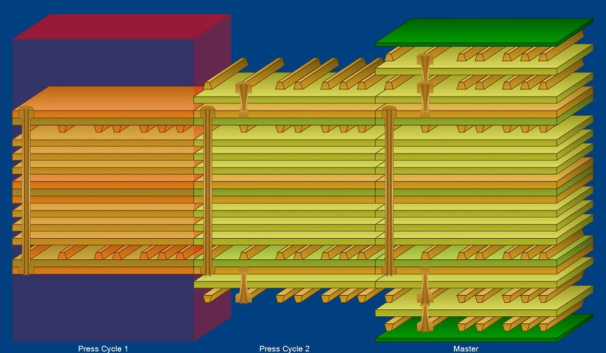
1. Sequential Lamination
In sequential lamination, HDI PCB stackups are created using blind, buried, and plated-through vias. The blind and buried vias have a smaller diameter, simpler model, and shorter via stubs than through-hole counterparts.
Sequential lamination manufacturing costs more than standard and lamination buildup. It is not suitable for high-density devices with multiple and large BGAs and fine pitch packages due to a limited number of layers allowed (a maximum of 2 to 3).
2. Standard Lamination
Standard lamination uses through-hole vias and is more limited in its application than sequential lamination stackup layers. The manufacturing process can be cheap for less than 20 to 28 layers, but for devices with multiple BGAs and fine-pitch components, the signal is difficult to route, and costs can add up. It also uses limited trace widths and thus is unreliable in its functioning and practicality.
3. Lamination Buildup
Lamination building using micro vias is one of the most preferred stackup types for HDI PCBs. In this type, the micro vias used have significantly smaller traces and dimensions that make them ideal for optimum signal routing even in fewer layers.
The micro vias can be stacked in different patterns, such as stacked or staggered, to increase space for routing. The increased space makes them perfect for large devices with multiple components and fine pitch packages.
Types of HDI PCB Stackups
Based on the manufacturing processes and the standards set by the IPC, there are a total of six types of HDI PCB stackup layers; I, II, III, IV, V, and VI. Only type I to III are considered suitable for HDI PCBs; the rest are costly to manufacture and have routing challenges.
Stackup Type I
The HDI stackup type I uses blind and through-hole vias. It has a laminated core with a single layer of microvias on one or both sides. The single microvia layer makes this stackup type unsuitable for large dense boards with multiple large BGA components and fine pitch pinpoints of less than 0.8mm.
The materials used, such as the thin FR-4 dielectrics, can cause delamination under extreme heat. Moreover, the aspect ratio should be less than 10, not the case here.
Stackup Type II
The HDI stackup type II also has a laminated core and uses blind, buried, and micro vias. It also uses a single layer of micro via on one or both sides, thus limiting its capabilities. The micro vias can only be placed on the outer layers, thus restricting ground and plane layers.
They are slightly better for use with high-density circuit boards, but the limited number of layers provides the same practical reliability that manufacturers cannot afford.
Stackup Type III
The HDI stackup type III uses a laminated core with blind, buried, and micro vias. The significant difference between stackup types I, II, and III is that it allows two or more micro vias on one or both sides of the circuit board. It is the most suitable stackup layer for a high-density circuit board with multiple fine-pitch BGAs.
The high-density board can have multiple layers, and PCB manufacturers can stack or stagger the micro vias based on the pattern and functionality required. Manufacturers can also use the outermost layers for ground and power planes and improve the signal integrity of the circuit board.
Type III stackup layer allow manufacturers to improve the signal integrity by using different design guidelines, such as via-in-pad or partial via-in-pad, and add more components on a single layer.
Other HDI PCB Considerations
Before designing an HDI PCB for your project, you should be aware of the costs and materials involved in the process. Depending on the number of layers and components, the process complexity can increase. This leads to the oveeerrrall cost increasing up to 50 to 80%.
In the end, you need to choose a stackup type that increases efficiency and improves signal integrity by using materials that can withstand high heat. The materials used in stackup type III are cost-effective and reliable but cannot be used in standard and sequential lamination processes.
The PCB manufacturers decided on the number of layer and stackup types based on the client’s routing density and signal integrity requirements. Thus, it’s best to consult a professional, like Hemeixinpcb.com, before designing a PCB layout.


