What is a blind microvia?
Via stands for vertical interconnect access. A via is basically a hole connecting two pads on two different layers of a PCB. The hole itself just provides an accesses from one pad to another. The conductivity is possible either through copper plating the hole between the pads or filling it with a conductor.
When this via is between the top or bottom layer (surfaces of the PCB) to one or more inner layers, it’s called a blind via. Though when a blind via goes beyond one inner surface, it is sometimes called a skip via. The word ‘blind’ refers to the fact that the via can only be seen from one side/surface of the PCB.
A blind via can never occupy an odd number of layers like starting with copper and ending on the substrate. Therefore, a blind via always connects an even number of layers: 2, 4, 6, and so on. And since a blind via cannot be from surface to surface, it is only possible in multilayer PCBs, with four or more layers.
It’s also important to note that most common blind vias are blind microvias. It’s possible to create conventional blind vias, but since the whole point of employing a blind via is to introduce compactness to the circuit, smaller and more compact blind microvias are generally preferred. They are a core element of HDI PCB technology.
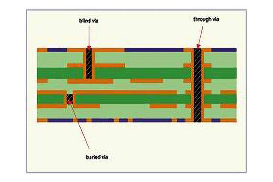
Blind Via
Let’s dive a bit deeper into the blind via (not possible since they are very shallow). Why are blind vias important, how are they formed, plated and filled, and what design rules should be followed while designing a PCB with blind vias.
Importance of Blind Via
Conventional PCB designs have relied primarily on PTH – Plated Through Hole vias. It is one of the reasons it is called the “standard via.” While it served the PCB industry well for decades, it has severe limitations. Despite still being useful for higher power components, PTH takes up a lot of space on a PCB, since a lot of PTHs need to be drilled. Therefore, it kills the compactness factor that is so important in modern PCBs.
Blind via, along with buried via, is a more subtle solution. Since it connects layers surface to layer rather than surface to surface, it helps save a lot of space in a PCB. Space that can be used for routing, and more components, thus reducing the size of the PCB. The need for blind vias arose, especially with the advent of SMT, and they are used for SMT pads most often.
By reducing the surface area needed that would have otherwise been occupied by PTHs, blind vias help increase the PCBs breakout channel. It also helps reduce the layer count in general.
Drilling a Blind Via
Making, or more accurately, drilling a blind via can be done by either a mechanical or laser drill, though the laser is much more commonplace. Mechanical drills are still chiefly employed for PTHs. For blind vias, mechanical drilling is sometimes employed for prototypes. But the via diameter usually doesn’t go beyond 0.1 mm.
Laser drilling is more efficient and simpler for making blind vias. Especially because you can control the aspect ratio more accurately for blind microvias, a single surface to the first inner layer via can be easily drilled with laser, but for blind via that needs to penetrate a number of layers, the process is different. A single layer blind via can be dissected into three elements, capture pad on the surface, target pad on the bottom layer, and plating that connect these two pads.
Now when you go for a multilayer blind via (or skip via), you either drill the hole through these layers (keeping in mind the aspect ratio), or you can drill through holes in each layer and then stack them together with sequential lamination. These holes then often need to be filled with a conductive filler material to dissipate heat.
Filling a Blind Via
In some cases, blind vias need to be filled with either a conductive or non-conductive material. It is important to note that the plugging or tenting of a via is different than filling or capping a blind via. Tenting (covering the via), or plugging (partial filling of the via) is usually reserved for PTHs. However, a blind via can be filled with either a conductive or non-conductive substance. It can also be capped or covered after being filled.
The conductive material used for filling a blind via is usually copper. Non-conductive Epoxy resin is usually chosen as the non-conductive filling. Conductive filling of blind vias is beneficial for high heat or high current transmission from layer to layer of an HDI. Copper filled microvias are ideal for high voltage HDIs. Epoxy filled vias are more common for via-in-pad requirements.
Important Notes about Blind Via
A designer has to keep some things in mind while designing with blind vias.
- Whether fabricator will use a mechanical (conical or standard) drill or a laser drill?
- Blind Microvia hole shape: Straight wall, cupped, negative/positive tapers, or some other shaped.
- Aspect ratio, especially with blind microvia.
- Designing techniques may vary if the fabricator is not using depth-controlled laser drilling.
- How many copper-filled layers you can use for stacked blind microvias.
These are just some of the factors a designer must consider while designing a PCB with blind vias. A more prudent approach would be to thoroughly understand the design guidelines provided by the manufacturer.
Merits and Demerits of Blind Vias
Like every other technology, a blind via has its own merits and demerits. Even though blind via is a technological advancement over conventional PTHs, they are still a costly option. For PCBs that don’t require too compact a design, blind vias can be an expensive substitute to PTHs. Also, blind vias that are supposed to penetrate more internal layers add to the cost.
There are many merits of blind vias. They help with a better footprint, compacting the circuit, improved BGA breakout, and better conductivity. Blind and buried vias improve the overall PCB design and have completely transformed the conventional PCB relying solely on PTHs.
Conclusion
The cost factor is still holding many PCB designers back from commonplace use of blind vias in their designs. For now, blind vias are mostly used where compactness of the circuit trumps its cost. But with laser drilling becoming more and more common, advancement in sequential PCB lamination, and improved stack up techniques, the cost may go considerably down.


