Via-in-Pad Design
A via-in-pad design places a tiny hole (called a via) directly in the center of a component pad. Think of it as putting a tunnel entrance in the middle of a busy road. It saves space and lets everything connect more directly.
This method is helpful when the circuit board is very crowded. Phones and compact industrial devices are the most common example of it. Via-in-pad design works well for BGAs (Ball Grid Arrays), which carries chip for integrated circuits.
However, the via-in-pad design changes how the board is built. The hole should be filled and the surface should be flat so parts can sit evenly. This is called planarization. If it’s not done right, solder can leak into the hole during assembly, which causes weak and unreliable connections.
Knowing when and how to use via-in-pad will help you build faster and more reliable boards. In this guide, we’ll explain the via-in-pad design rules, benefits, and challenges of using this technique in your projects.
Material Selection for High-Reliability Via-in-Pad
Designs
The materials selection is very important when using via-in-pad in industrial and high-speed circuit boards. These boards often face heat, vibration, and fast electrical signals, so the materials should be capable enough to hold up well under stress.
The first thing to check is the board’s insulation. It is called the dielectric material. It needs a low coefficient of thermal expansion (CTE). This means it won’t expand or shrink too much when the board heats up or cools down. If the CTE is too high, it can stretch the via and cause cracks in the copper over time.
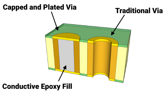
Copper is the best choice for filling the via holes as it conducts electricity and heat well. For simpler boards that don’t need high performance, manufacturers also use non-conductive epoxy.
Prepregs are the core and bonding layers of the board. Manufacturers need to make sure that prepregs also match in strength and heat resistance with the material. If they don’t, the layers will shift apart during the high-pressure heat cycles used in manufacturing.
PCB Stack-Up Optimization for Via-in-Pad Structures
Planning the layer structure of your PCB, called the “stack-up,” is very important when using via-in-pad. This is especially true for boards that carry fast signals.
Via-in-pad simply means the hole (via) is placed in the spot where an electrical component connects to the board. In order to keep the board stable, designers need to make sure that the layers underneath are arranged properly.
A well-designed stack-up helps in many ways:
- It keeps the board flat
- Controls how signals travel (impedance)
- Protects the vias from damage when the board heats up and cools down
The stack-up also has to match the depth of the drilled holes with the thickness of the board. If the holes aren’t of the perfect size, they can crack or fail over time.
Manufacturers make the layer stack symmetrical, similar to a sandwich with the same layers on each side. This helps prevent bending or warping of the delicate PCB.
Plating and Metallization Techniques for ThermoMechanical Robustness
Plating and metal coating are important for making vias strong. Metallization is especially required when the vias sit directly under parts. To make the vias work properly, the walls of the holes are coated with copper, as copper can act as a strong, electrical bridge between the layers.
In boards that must last a long time and work in tough conditions, the copper needs to be thick and evenly spread. If the copper is thin or rough, it can crack when the board undergoes temperature changes. It is similar to how thin water pipes burst when the water inside freezes and expands.
To make better copper layers, manufacturers use electrolytic plating and pulse plating. These techniques fill the via walls evenly and reduce air gaps.
In via-in-pad designs, the plated hole is filled with copper for heat flow and better strength, or with epoxy for simpler jobs where the stress is lower. After smoothing out the surface, a final coating of ENIG (Electroless Nickel Immersion Gold) is added to protect the copper and make soldering easier.
Simulation and Modeling of Thermal Cycling Effects on
Via-in-Pad
Engineers use simulation and modeling to predict how via-in-pad designs will handle heat and stress over time.
Thermal cycling happens when a circuit board keeps heating up and cooling down again and again. Just like roads can crack from hot days and cold nights, circuit boards also get stressed from this repeated change. Different materials used inside the circuit board expand and shrink at different rates. This can stretch and squeeze the copper inside the vias.
This is where the coefficient of thermal expansion (CTE) comes into the equation. If copper and the surrounding layers in the PCB have different CTEs, the via walls will crack and separate over time.
To study these effects, engineers use finite element analysis (FEA). It creates a virtual model of the via-in-pad and simulates how stress builds up when the board is going through varying temperatures.
Experimental Testing of Via-in-Pad Reliability
Testing via-in-pad reliability allows engineers to check how well the electrical components on the board can hold up to real-world stress. These tests spot problems before the board is used in machines or equipment.
One common test is thermal cycling. In this test, the circuit board is heated and cooled repeatedly. Thermal cycling reveals bending of the copper (called barrel fatigue), cracks in the via, and pads that lift off the surface.
Another method that the engineers use is cross-section analysis. It is a technique in which engineers cut the printed circuit board to look inside a via using a microscope. They check:
- How thick is the copper plating
- Whether the fill is solid
- If there are any tiny defects that could cause failure later
X-ray inspection is also used to see inside the via. This method saves the board from being cut into pieces. X-rays can find hidden air pockets (voids) and parts that are not lined up correctly.
Lastly, manufacturers conduct mechanical tests and electrical continuity before giving a green signal for the production of the PCBs.
Impact of Via Filling Materials on Thermal Reliability
There are two main types of material fill: conductive and non-conductive.
Conductive fill is usually made of copper. When used in a via, it helps spread heat away from hot electrical components. Copper keeps the board cooler and prevents damage. It also adds strength to the via and reduces the chance of cracks.
Non-conductive fill is made from a type of plastic called epoxy. Epoxy is cheaper and easier to work with, but it doesn’t carry heat. It also expands at a different rate than copper, which puts stress on the via walls. Over time, this can lead to delamination.
The fill material also has an effect on how easy it is to attach components to the PCB. Copper creates a flat surface that’s great for soldering. On the other hand, epoxy fill needs extra work to make the surface even and reliable for mounting tiny electrical parts. Hence, copper is the first choice of manufacturers working on high-performance circuit boards.
Design Guidelines to Improve Via-in-Pad ThermoMechanical Reliability
These are some design rules that engineers implement to improve via-in-pad thermomechanical reliability:
1. They use copper to fill the via as copper carries heat well and allows the machine to run all day without any problems.
2. They make the copper plating inside the via thick so that the walls have more support and don’t wear out over time.
3. They keep the via's shape strong by keeping the aspect ratio low. In simple words, the ratio means how deep the hole is compared to how wide it is. A good target is 10:1 or less.
4. They don’t put vias too close to the circuit board’s edge or near moving/shaking parts. These spots get more physical stress, and a via there would crack easily.
5. They use pad sizes that are big enough to hold soldering. If they’re too small, the electronic components would not stick well, and soldering would fail.
Case Studies in High-Reliability Applications
(Aerospace, Automotive, and 5G Infrastructure)
Via-in-pad design has been a proven success in industries that can’t compromise on the reliability of PCBs. This method improves how the board handles heat, vibration, and fast signals. Here are some real-world examples to give you an idea of how it works in action:
|
Sector |
Application |
Via-in-Pad Benefit |
Example |
|
Aerospace |
Via-in-Pad is used for avionics and satellite boards |
Reduces weight and improves signal integrity in compact multilayer stack-ups |
NASA avionics systems use via-in-pad to meet SWaP (Size, Weight, and Power) goals |
|
Automotive |
You’ll find Via-in-Pad in Advanced Driver-Assistance Systems (ADAS) and ECU modules |
It enhances reliability under high thermal cycling and vibration |
Tesla and Bosch use filled via-in-pad in ECUs for thermal and vibration resilience |
|
5G Infrastructure |
High-frequency RF modules and antenna arrays work smoothly in Via-in-Pad setup |
It improves impedance control and minimizes signal loss at mmWave frequencies |
Qualcomm and Verizon use via-in-pad in mmWave 5G hardware for high-speed, compact RF designs |
Industry Standards and Guidelines for Via Reliability in
Thermal Cycling
IPC-2226 and IPC-6012 are the two industry standards that ensure vias stay strong during drastic temperature changes.
IPC-2226 and IPC-6012 standards give clear rules about:
- How big should the vias be
- How thick does the copper plating need to be
- What materials to use
This prevents problems like cracking and layers coming apart in the long-term use.
Manufacturers' main focus is to reduce differences in how much copper and the surrounding materials expand and shrink with temperature changes. A cracking printed circuit board under stress is the worst nightmare of engineers.
The IPC guidelines also have testing protocols for thermal cycling. A PCB prototype cannot go into production until it verifies its via durability in real conditions. For via-in-pad designs, these standards specify minimum via sizes and plating requirements to maintain the mechanical strength of the board.
These guidelines cannot be ignored by manufacturers who supply printed circuit boards to the aerospace and automotive industries.
Conclusion
Via-in-pad design is very important for making fast-working PCBs. They are especially useful in tough industrial scenes and high-speed electronics.
Choosing the right materials, using good plating methods, and following design rules all help the PCB handle heat and mechanical stress well. If you want professional help with advanced via-in-pad manufacturing, check out Hemeixin. We have the expertise to help you make your projects and devices market-ready!


